
Tutorials
FPGA Pulse Synchronizer: Transfer Events Without Silently Losing Them
Published · Updated
A source pulse can rise and fall between two destination-clock edges. Passing it through a level synchronizer may therefore produce no destination event at all. Start by deciding whether the system must preserve every event, then check the transfer mechanism’s rate and reset contract.
A narrow pulse can disappear without a logic error
Consider a source event that stays high for 10 ns while the destination samples every 40 ns. Depending on phase, no destination edge may see it high. Adding more destination synchronizer stages does not recover a transition that the first stage never sampled. This is a sampling problem before it becomes a latency problem.
The illustration uses ideal clocks to show the missed-pulse case. Real crossings also face metastability around sampling edges. A waveform that happens to pass in one simulation phase is weak evidence; vary clock phase, frequency ratio and event spacing. A single-bit level synchronizer fits a stable status contract, not arbitrary event counting.
A toggle-based transfer encodes an event as a state change, which can persist long enough to be observed. But two source toggles before the destination observes the intermediate state can cancel as far as the receiver is concerned. If the source cannot respect a minimum event spacing, use a protocol with backpressure or an appropriately sized event/data queue.
Calculate the documented XPM pulse gap
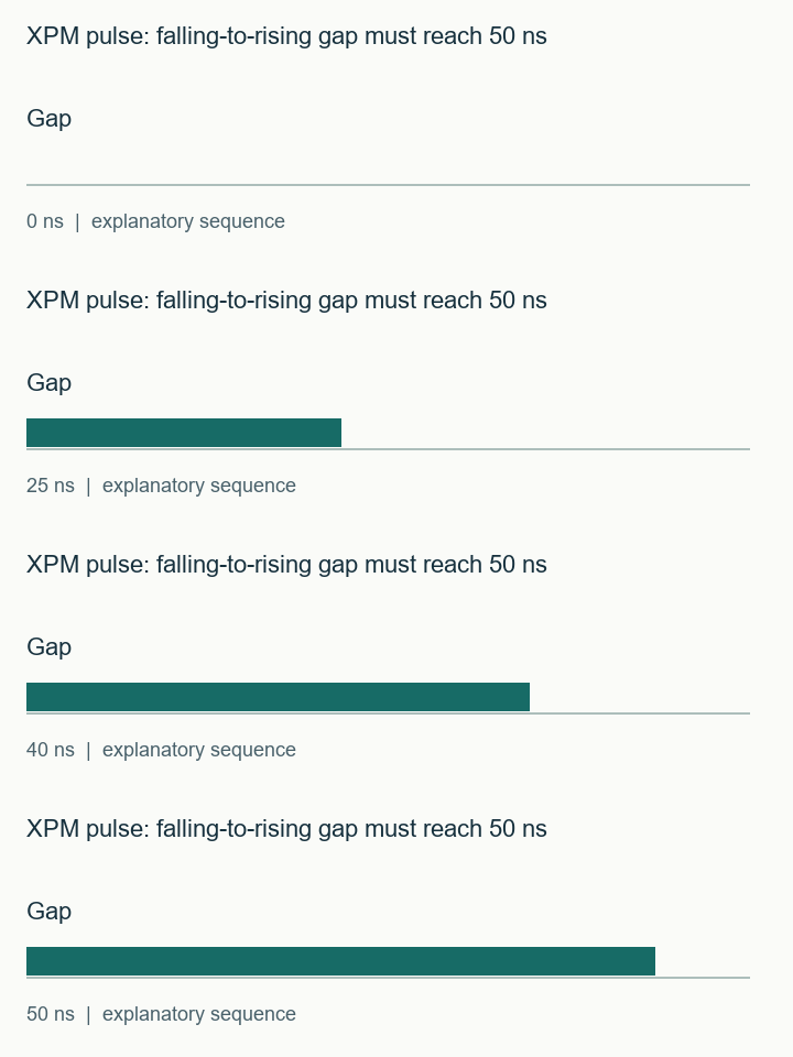
For XPM_CDC_PULSE in UG953 2024.1, the minimum input gap is twice the larger source or destination period. Measure it from the previous source pulse’s falling edge to the next pulse’s rising edge. With a 10 ns source period and 25 ns destination period, the required gap is 50 ns. A 10 ns-wide pulse plus that gap gives a 60 ns minimum start-to-start interval for this example.


The macro produces a destination pulse one destination period wide when its input contract is met. Its output is combinational unless REG_OUTPUT is set to 1. Use the installed macro template and review all selected parameters. The calculator here checks the documented spacing arithmetic; it does not simulate the vendor macro.
The logic-analyzer photograph shows an instrument’s internal board, not a captured trace from this example. At the bench, count source and destination events over the same test interval. A plausible-looking isolated pulse says little about event loss during a burst. Add an event sequence or counter when you need an observable loss check.
For a stream that includes data with each event, revisit the buffering and backpressure requirements; the acquisition-buffer example shows why average rate alone does not describe a burst.
XPM pulse spacing and reset calculator
Inputs and exported records stay in this browser. The check evaluates the assumptions you enter; it does not inspect your project files.
Use the worked values and equations above, or download the examples below. The interactive check requires JavaScript.
Reset the transfer logic as one protocol
When the optional XPM pulse resets are used, UG953 requires simultaneous assertion of source and destination resets for at least (DEST_SYNC_FF + 2) × Tdest + 2 × Tsrc. With four destination stages, 25 ns destination period and 10 ns source period, that is 170 ns. Do not toggle the source pulse during reset; ignore the destination pulse then.
This macro-specific reset contract is more than simply adding a local reset synchronizer to each side. Coordinate the complete transfer protocol, including startup and any clock-stop condition. If resets are disabled, the documented feedback implementation cannot recover from an undefined source-pulse value propagating through it.
Test an event just before reset, during reset suppression and after restart. Define whether an in-flight event is discarded, retried or acknowledged. Otherwise, a system can count correctly in steady state and still duplicate or lose an event at startup.
Use the tool to compare the available falling-to-rising gap with the minimum and export the reset interval. Its results are design inputs, not CDC certification. Complete the coverage audit and inspect the timing-exception scope for the actual implementation.
Watch the short xpm pulse: falling-to-rising gap must reach 50 ns sequence
The sequence visualizes the stated example. It is not a hardware capture. The static figures and text above contain the same explanation.
Export the rate assumptions and reset contract, then include a source/destination event-count trace in your review.
Download the timing and RTL examples (ZIP) · Discuss this engineering task
The ZIP includes the clock and I/O examples, timing-audit commands, counter/latch/reset RTL and testbenches. Bring the relevant exported record to the enquiry; this page does not submit it automatically.
References and example scope
Documentation checked 16 November 2026. AMD examples use the cited 2024.1 documentation baseline. Vivado commands and vendor macros were not executed for this article. Counter, latch and illustrative reset tests were executed with Icarus Verilog; latch structure was checked with Yosys. See the included commands and validation record for the exact scope.