
Tutorials
I2C Pull-Up Resistor Calculation: Find a Range That Meets Both Limits
Published · Updated
Calculate a permitted interval, not a favourite resistor
An I2C pull-up must be weak enough for a device to pull the line low and strong enough for the line to rise in time. Start with the bus supply, allowed low-level voltage, guaranteed sink current, permitted rise time and estimated total bus capacitance. Use compatible units and keep the conditions of the sink-current specification.

For the simple RC model, Rmin=(VCC−VOLmax)/IOL and Rmax=tr/(0.8473×Cb). The rise-time expression refers to the 30%–70% interval used by this model. It is not the time from zero to the full supply voltage. Buffers or rise-time accelerators can require a different analysis.
Board bring-up sequence: Prepare the board checks before testing this interface.
I/O count and allocation: Reconcile signal count and physical allocation.
Work through a feasible range and an empty range
For an illustrative 3.3 V bus, VOLmax=0.4 V, IOL=3 mA, tr=300 ns and Cb=100 pF, the limits are approximately 967 ohms and 3.54 kilohms. Those are calculated bounds under the stated assumptions, not a recommendation for an unidentified FPGA pin. Check every connected device and the selected bus mode.
Double the capacitance and the upper bound halves. Eventually it can fall below the lower bound. That is an inconsistent requirement set; choosing the midpoint does not fix it. Revisit loading, bus speed, segmentation or the interface architecture, then recompute with the revised assumptions.
External input/output timing: Include the external path in the timing budget.
Clock-domain synchronization: Keep asynchronous sampling separate from interface logic.
Include parallel pull-ups and resistor tolerance
Several modules may each contain a pull-up. Their parallel equivalent can be much lower than the resistor visible on the main schematic. Two 4.7 kilohm pull-ups make 2.35 kilohms before tolerance. Count pull-ups on both SCL and SDA, including optional assembly variants.
Evaluate the resistance extremes against both limits: the smallest equivalent resistance challenges low-level drive, while the largest challenges rise time. Save the capacitance estimate and its uncertainty with the result. During validation, measure rise time at an appropriate threshold and check low voltage under the relevant load. The calculator is a starting budget; it does not establish signal integrity from nominal values alone.
Power-on test record: Retain the power states and test sequence.
Use the equations and review steps above. Interactive checks require JavaScript.Watch the short worked pull-up window sequence
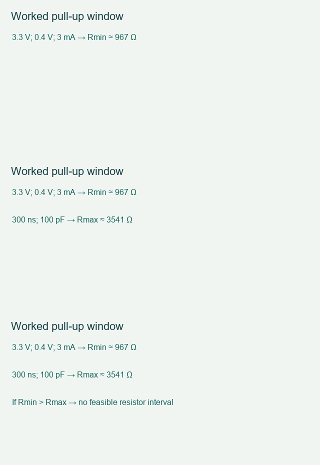
Save the check result with your exact device, board revision and unresolved conditions. Discuss the interface requirements when the remaining issue needs a board or implementation review. Opening this link does not submit the worksheet.
Sources and example scope
Documentation checked 17 November 2026. Worked values are illustrative calculations. No board measurement or Vivado implementation run is claimed. The worksheet checks entered assumptions and does not inspect your schematic or project files.
Back to Tutorials