
Tutorials
FPGA SPI CPOL and CPHA: Check the First Bit Before Decoding a Byte
Published · Updated
Identify idle level and the first sampling edge
SPI mode selection becomes easier when the first edge is visible. CPOL describes the idle clock level. CPHA selects whether sampling occurs on the first or second clock edge of a bit period. Write those two facts beside the peripheral timing diagram before choosing a mode number.

Mode 0 and mode 3 both sample on a rising edge, but their idle levels and first-edge behavior differ. “Rising-edge SPI” is therefore not a complete interface specification. With CPHA equal to zero, the first data bit must already satisfy the receiver setup requirement before the first sampling edge.
Board bring-up sequence: Prepare the board checks before testing this interface.
I/O count and allocation: Reconcile signal count and physical allocation.
Inspect CS and the first bit before the decoded byte
Capture CS, SCLK and the data line together. Check the idle clock level before CS becomes active, the first edge after selection, and when the first data bit becomes valid. Only then compare the decoded byte. A decoder configured to the same wrong assumption as the RTL can make a waveform look more convincing than it is.
Choose a test pattern with transitions at useful positions rather than relying only on all-zero or all-one data. Keep bit order and word length explicit. Also inspect the final bit and CS release: a correct first byte does not prove that back-to-back transactions meet the peripheral selection and deselection requirements.
External input/output timing: Include the external path in the timing budget.
Clock-domain synchronization: Keep asynchronous sampling separate from interface logic.
Separate mode mismatch from missing timing margin
If lowering SCLK changes the result, inspect source output delay, board delay and receiver setup/hold requirements. A mode change is not a substitute for an external timing budget. A translator or long route can consume margin without changing the nominal CPOL/CPHA relationship.
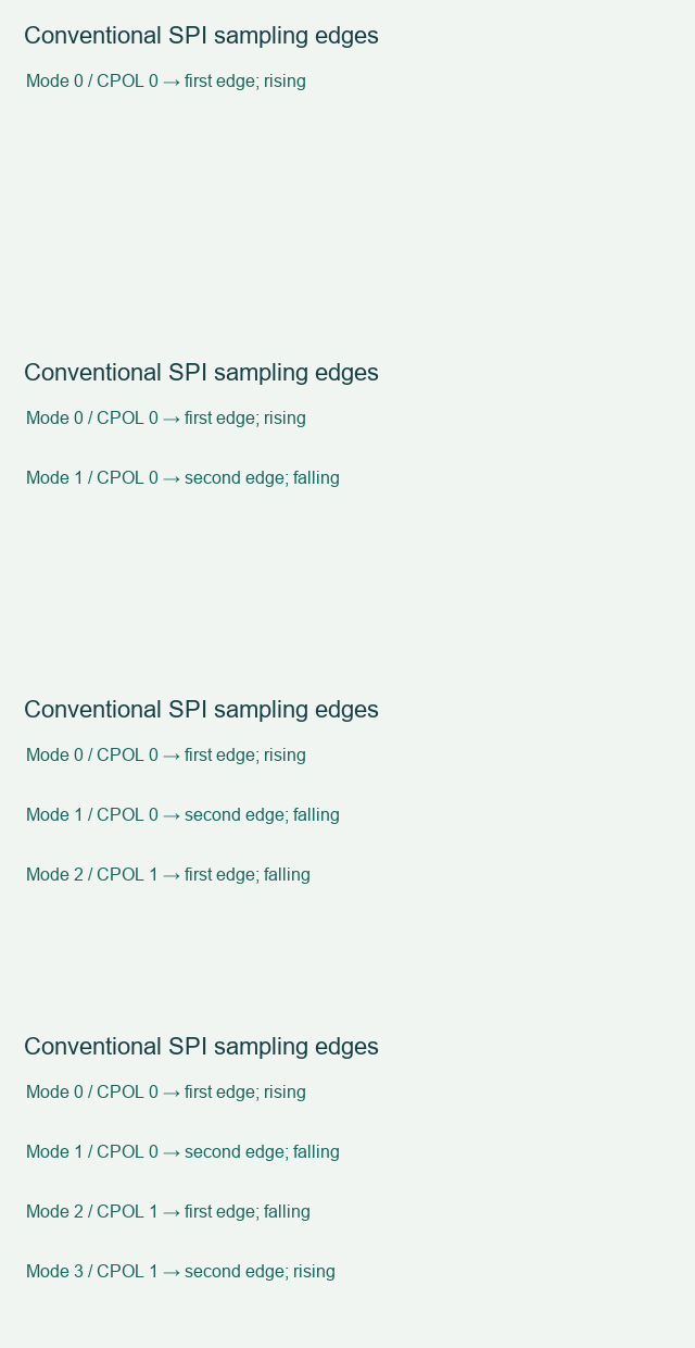
The selector below gives the four conventional edge mappings. It does not select the mode required by an unknown peripheral. Export your selected mode with the device timing-page reference, CS limits and measured clock rate. When using an FPGA-generated SCLK, keep the design clocking and I/O constraints consistent with the actual implementation rather than treating the interface as an unconstrained slow signal.
Power-on test record: Retain the power states and test sequence.
Use the equations and review steps above. Interactive checks require JavaScript.Watch the short conventional spi sampling edges sequence
Save the check result with your exact device, board revision and unresolved conditions. Discuss the interface requirements when the remaining issue needs a board or implementation review. Opening this link does not submit the worksheet.
Sources and example scope
Documentation checked 17 November 2026. Worked values are illustrative calculations. No board measurement or Vivado implementation run is claimed. The worksheet checks entered assumptions and does not inspect your schematic or project files.
Back to Tutorials