
Tutorials
FPGA Reset Synchronizer: Release Each Clock Domain Cleanly
Published · Updated
A reset can assert immediately while its release is made synchronous to a destination clock. That arrangement still needs a defined reset polarity, a running clock and a startup contract for the logic it controls. One reset net does not mean every clock domain leaves reset together.
Treat the reset source and local release separately
A pushbutton is a physical input, not a clock-domain policy. The photograph shows a tactile switch on a consumer control board; it is not an FPGA reset circuit. A real reset source may instead be a supervisor, another device or a software-controlled signal. Check its polarity, pulse duration, electrical behavior and behavior during power transitions.


Mechanical switch bounce is a separate issue from synchronized release. Repeated assertions can repeatedly reset a design even when each release is synchronized correctly. Similarly, a clock that has not started cannot advance a release chain. Include these conditions in the startup investigation rather than treating the synchronizer as a universal reset conditioner.
AMD documents XPM_CDC_ASYNC_RST for asynchronous assertion and destination-synchronous deassertion. Use the macro and device documentation for the production implementation. The small two-stage RTL below is an educational behavior example with active-high reset, not a vendor-macro replacement.
Read a two-stage release one edge at a time
(* ASYNC_REG = "TRUE" *) reg [1:0] pipe;
always @(posedge clk or posedge arst)
  if (arst) pipe <= 2'b11;
  else pipe <= {pipe[0],1'b0};
assign rst = pipe[1];
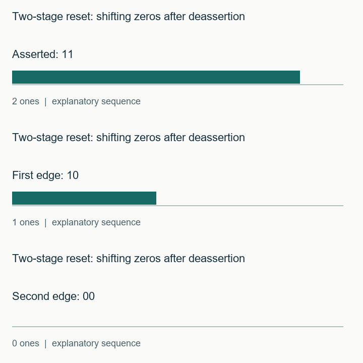
Assertion fills the chain with ones without waiting for a clock edge. After arst goes low, the first rising clock edge shifts in one zero; rst remains high. The second rising edge shifts the second zero through, and rst becomes low. The consumer observes the released reset according to its own sequential sampling. Do not describe that behavior as “the whole chip starts on the second edge.”
The supplied testbench asserts reset between edges, releases it before the next edge, checks that release is not early, then reasserts it. It passed in Icarus Verilog from OSS CAD Suite 2026-11-15. This verifies the RTL event behavior. It does not model metastability, prove recovery/removal timing or establish a physical minimum reset pulse width.
Follow the selected device’s minimum pulse requirements and implementation guidance. ASYNC_REG is an implementation attribute; it does not turn a failing physical reset source into a valid one. For the receiving clock itself, verify the clock definition and report.
Release each domain, then enable communication
Create a reviewed local release path for each relevant destination clock domain. Clock A and clock B may exit reset at different wall-clock times. If one domain can issue a request before the other is ready, the interface must tolerate that state or hold requests until readiness is established.
A local “out of reset” flag crossing to another domain is itself a CDC signal. Define whether the receiver needs a stable readiness level or an event. Use the level-crossing guide or the pulse-transfer contract accordingly. Coordinating reset is part of the interface design, not an afterthought to the reset wire.
Estimate local release without hiding clock assumptions
The release calculator shows the ideal digital delay from a known deassertion phase: time to the next edge plus the remaining chain intervals. The phase is defined here as time elapsed since the previous rising edge. Its range excludes the exact edge; physical behavior near that edge requires a metastability analysis that this calculator cannot provide.
Record stopped-clock behavior and the first transaction after restart. Include those checks in the board bring-up plan. Export the local release assumptions with the clock-domain map when requesting review.
Ideal reset-release timing worksheet
Inputs and exported records stay in this browser. The check evaluates the assumptions you enter; it does not inspect your project files.
Use the worked values and equations above, or download the examples below. The interactive check requires JavaScript.
Watch the short two-stage reset: shifting zeros after deassertion sequence
The sequence visualizes the stated example. It is not a hardware capture. The static figures and text above contain the same explanation.
Download the RTL test and export the clock-domain release assumptions for a startup review.
Download the timing and RTL examples (ZIP) · Discuss this engineering task
The ZIP includes the clock and I/O examples, timing-audit commands, counter/latch/reset RTL and testbenches. Bring the relevant exported record to the enquiry; this page does not submit it automatically.
References and example scope
Documentation checked 16 November 2026. AMD examples use the cited 2024.1 documentation baseline. Vivado commands and vendor macros were not executed for this article. Counter, latch and illustrative reset tests were executed with Icarus Verilog; latch structure was checked with Yosys. See the included commands and validation record for the exact scope.