
Tutorials
Single-Bit Clock Domain Crossing: When a Synchronizer Is Enough
Published · Updated
A slowly changing status flag and a one-cycle event are both one bit wide, but they need different clock-domain-crossing treatment. A level synchronizer is a candidate when the receiving logic needs a stable state and can tolerate latency. Width alone is not enough to choose it.
Write down what the receiving logic must preserve
For a “link ready” flag, the receiver may only need the eventual asserted or deasserted state. For “one sample completed,” every event may matter. For an eight-bit command, the bits may have to arrive as one coherent value. These are different contracts even when the source logic looks simple.


The Parallella photograph illustrates a board with several connected devices. It does not establish which signals are asynchronous or which synchronizer those interfaces use. Build the domain map from RTL, clock generation and interface documentation, not from the number of chips in a photograph.
Record the source domain, destination domain, meaning of each transition and maximum change rate. If losing a transition changes a count, use the event-transfer discussion. If multiple bits form a value, choose a reviewed handshake, Gray-code scheme where appropriate, or asynchronous FIFO. Independent bit synchronizers do not provide bus coherence.
Keep the first synchronizer stage away from functional logic
A conventional destination synchronizer gives a potentially metastable first stage time to settle before later stages drive ordinary logic. Functional logic must not also consume that first stage. Register the source when the architecture requires a clean source-domain level; combinational glitches create extra transitions that the receiving circuit was not meant to interpret.
For AMD 7-series designs, XPM_CDC_SINGLE provides a documented macro with a configurable destination chain and optional source input register. The 2024.1 guide permits DEST_SYNC_FF values from 2 through 10, with 4 as the default. The correct choice depends on reliability and timing requirements; “two flops” is not a universal reliability guarantee.
Use the macro template supplied for your installed Vivado version and inspect the resulting CDC report. This article does not provide a substitute implementation of XPM_CDC_SINGLE. The architecture drawing below is conceptual; its arrows do not imply a fixed cycle latency or a measured metastability rate.
Keep the chain recognizable to the tools and review placement and constraints. A clean RTL simulation can check logical behavior, but ordinary digital simulation does not reproduce the analog metastability resolution process. The Vivado tools entry is a starting point for the implementation environment.
Review reset, reconvergence and the next consumer
Trace the synchronized signal into the consuming logic. Two separately synchronized copies can become visible on different cycles; reconverging them can create a combination that the designer did not expect. Prefer a single reviewed crossing point and then distribute the destination-domain result where the architecture permits it.
Also check startup. What does the consumer do before the synchronized status becomes valid? If it must remain idle, make that an explicit state or enable condition. Use the reset-release discussion to define startup independently for each clock domain.
Choose the crossing from its information contract
The decision aid asks about meaning, width and event preservation. A “candidate” result means that a level synchronizer fits the stated information contract; it is not a CDC sign-off. Unknown source behavior remains unresolved. Export the contract and compare it against the RTL and report.
Pair the CDC review with timing coverage and the exception review. Removing timing analysis between unrelated clocks does not validate the crossing structure or its functional protocol.
Single-bit crossing decision aid
Inputs and exported records stay in this browser. The check evaluates the assumptions you enter; it does not inspect your project files.
Use the worked values and equations above, or download the examples below. The interactive check requires JavaScript.
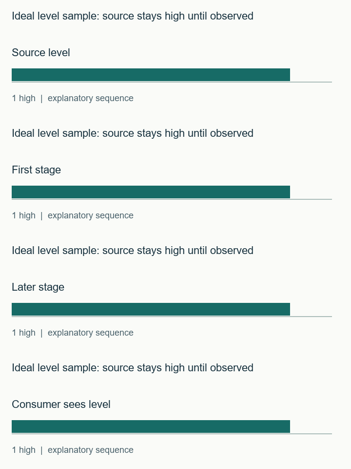
Watch the short ideal level sample: source stays high until observed sequence
The sequence visualizes the stated example. It is not a hardware capture. The static figures and text above contain the same explanation.
Export the signal contract and attach the relevant RTL and CDC report when requesting a crossing review.
Download the timing and RTL examples (ZIP) · Discuss this engineering task
The ZIP includes the clock and I/O examples, timing-audit commands, counter/latch/reset RTL and testbenches. Bring the relevant exported record to the enquiry; this page does not submit it automatically.
References and example scope
Documentation checked 16 November 2026. AMD examples use the cited 2024.1 documentation baseline. Vivado commands and vendor macros were not executed for this article. Counter, latch and illustrative reset tests were executed with Icarus Verilog; latch structure was checked with Yosys. See the included commands and validation record for the exact scope.