
Tutorials
AD7606 and Artix-7 Data Acquisition Throughput and Buffer Budget
Published · Updated
Before choosing an FPGA for an AD7606 acquisition system, calculate the stored payload and the data that accumulates while the output pauses. Then check interface timing, voltage domains, usable memory, and implementation constraints separately. This article uses the original eight-channel, sixteen-bit AD7606 for a worked budget and an Artix-7 device as a candidate to investigate. It does not provide validated RTL, prove a device fit, or report a tested acquisition board.
Freeze the ADC Variant and Acquisition Requirement
Write the complete ADC identity into the requirement. The original AD7606, its channel-count variants, and later AD7606B or AD7606C devices must not be treated as one interchangeable specification. This worked example concerns the original eight-channel AD7606 described in Analog Devices' Rev G data sheet and product documentation, with up to 200 kSPS on all channels. Recheck the exact ordering code and operating conditions before using those limits in a design.
Define a frame as one stored group of channel results from an acquisition event. Specify the number of stored channels, frames per second, bits stored per channel, and any metadata added per frame. Decide whether the stored representation preserves the raw ADC words or adds padding, timestamps, status, and sequence identifiers. The payload budget must follow the representation actually transported and stored, not merely the converter's nominal resolution.
Define the output behavior as carefully as the sampling behavior. Is the destination continuously available, occasionally stalled, or disconnected for long periods? Can sampling pause, or must the design retain every frame during a specified interruption? What should happen when a buffer fills? These questions determine memory requirements and failure policy. “USB output” or “Ethernet output” alone does not specify the guaranteed service available to the acquisition pipeline.
Separate digital transport requirements from analog performance. Correct framing and no detected queue overflow do not establish input accuracy, settling, noise, bandwidth, reference quality, or channel behavior. Those need a separate analog design and verification plan. Likewise, a catalogue entry for an Artix-7 candidate does not establish pin compatibility, resource fit, or timing closure. The first useful deliverable is a bounded requirement that makes each of those later checks possible.
Calculate Payload Before Choosing the Interface
For this worksheet, each channel occupies a whole number of bytes: round stored bits per channel up to the next multiple of eight. Multiply that byte count by the channel count, then add frame overhead. Multiply bytes per frame by frames per second to obtain bytes per second. This model deliberately does not pack arbitrary-width samples across byte boundaries. If the implementation uses a different packing rule, calculate that format explicitly.
With eight channels, sixteen bits per channel, no additional frame overhead, and 200,000 frames per second, each frame contains sixteen bytes. The payload is 3,200,000 bytes per second, or 3.2 decimal MB/s. Multiplying by eight gives 25.6 Mbit/s. These are application payload figures. They are not a minimum serial-clock specification, an achieved host-transfer rate, or proof that a particular serial or parallel interface meets timing.
To select the acquisition interface, use the exact data sheet's timing diagrams and operating conditions. Account for the available read window, serial output arrangement or parallel bus behavior, control timing, and any restrictions on overlap with conversion. Then check the FPGA's input timing and implementation. A payload-rate division that ignores the read window and protocol details can substantially misrepresent the required interface speed.
Budget the output protocol separately. Headers, checksums, alignment, packet boundaries, software buffering, and intermittent host service can reduce effective delivered throughput. Measure or otherwise establish application-level service for the chosen output implementation. If the average sustainable output rate is no greater than the acquisition input rate, finite buffering cannot make continuous operation stable indefinitely. The calculator does not include an output-service model, so this requirement remains an explicit follow-up check.
Size Buffers for Output Stalls
For an initially empty buffer and a complete output pause, incoming bytes accumulate at input rate multiplied by pause duration. At the worked payload rate, a ten-millisecond pause adds 32,000 bytes; a one-hundred-millisecond pause adds 320,000 bytes. These are decimal byte counts before engineering margin and before any initial occupancy. The tenfold increase in pause duration produces a tenfold increase in required temporary storage.
The worksheet adds a user-selected percentage margin to that accumulated data and rounds the result up to a whole byte. This margin is a planning allowance, not a substitute for knowing the maximum pause. If the buffer already contains data when the pause begins, add that initial occupancy separately. If input arrives in bursts, include the burst bound. A system with overlapping queues needs a clear explanation of which queue absorbs each interruption.
After service resumes, the output must drain the backlog while new samples continue arriving. Determine how quickly the backlog clears and whether another stall can occur first. For a constant output service greater than input, the net draining rate is output minus input. Divide the backlog by that net rate for a simple recovery-time estimate. Real packet and scheduling behavior may require a more detailed model, but the calculation exposes why matching average input exactly is insufficient for recovery.
Compare the required storage with usable implemented memory, not only an advertised total bit count. FIFO width, depth, block granularity, metadata, clock-domain crossing, other design users, and reserved capacity affect the mapping. Use the BRAM budget tool for an initial estimate, then inspect synthesis and implementation reports for the selected part. A 320,000-byte requirement should remain a requirement to map and verify, not become an unsupported statement that the named Artix-7 package can accommodate the complete design.
Interactive planning worksheet
The worked method remains in the article. JavaScript adds input fields and a local summary export; no data is submitted.
Check I/O Banks Clocks and Voltage Domains
Create an interface table listing every ADC data and control signal, direction, timing relationship, electrical domain, and FPGA pin assignment. The original AD7606 documentation separates its analog supply from its digital interface supply. Review the chosen interface supply against the FPGA bank's permitted I/O standards and operating conditions. Do not connect a signal based only on a nominal “3.3 V compatible” label without checking the exact requirements and board power arrangement.
Choose serial or parallel operation only after considering the pin budget and timing. A wider bus can consume more pins and routing resources, while a narrower interface can demand a different timing solution. Include control, reset, mode, and clock-related signals in the count. Use the I/O budget tool to organize totals, then map them to the exact package and bank resources. Family-level maximum I/O counts are not package assignments.
Identify clock domains and crossing points. Conversion control, ADC readout, buffering, and host output may not share one timing relationship. Synchronize control information appropriately and use a reviewed method for transferring multi-bit data between domains. An asynchronous FIFO is one possible architectural element, but its correctness depends on implementation, constraints, reset behavior, and verification. Naming the block does not establish that the crossing is safe.
Preserve measurement access for bring-up. Plan where to observe conversion control, completion indication, read activity, and output backpressure without excessively loading the circuit. Keep the schematic, constraints, and test-point references aligned. Before applying signals, review powered and unpowered behavior of both devices. The block diagram in this article intentionally avoids unverified ball numbers, board-specific termination values, or a universal clocking recipe. Those decisions belong to the actual hardware design and its documented limits.
Partition RTL and Define Simulation Checks
Partition the digital path into responsibilities: conversion scheduling, ADC interface sequencing, channel-word capture, frame assembly, buffering, and output delivery. Give each boundary an explicit contract. For example, define when a frame becomes valid, whether it can be stalled, how its sequence identifier advances, and what happens on reset. A clear contract makes simulation failures easier to localize than one large state machine with implicit assumptions.
Use a testbench source that supplies known channel patterns and exposes ordering mistakes. Different values for each channel and frame can reveal duplication, omissions, and swapped channels that a constant input would hide. Verify frame length and metadata as well as sample words. Include reset during idle, reset during transfer, delayed completion, and output backpressure cases that the design is expected to handle. These are proposed checks, not simulation results supplied with this article.
Define overflow behavior explicitly. If sampling cannot pause and storage fills, the design must expose that condition and apply the agreed policy. A sticky status bit, dropped-frame count, or new recording segment can make the event visible to software. Choose the mechanism according to the application, and test how it is cleared or acknowledged. Avoid presenting an apparently continuous sequence after silently discarding data.
Check timing constraints and implementation reports in addition to behavioral simulation. A functional testbench does not prove external setup and hold compliance or clock-domain crossing correctness. Tie constraints to the exact board and data-sheet timing assumptions. Review resource usage after integrating output logic and other system blocks, not only the acquisition module in isolation. Keep build and constraints revisions with the reports so that a later parameter change cannot inherit an obsolete timing-closure claim.
Export the Acquisition Design Brief
Export the frame format, input rate, assumed maximum output stall, margin, and resulting buffer requirement. State that the calculator assumes an initially empty buffer and complete lack of output service during the entered pause. Add initial occupancy, burst effects, and output recovery requirements in the design record. If those values are unknown, record them as questions to resolve rather than selecting a small convenient pause to make the memory budget fit.
Attach the exact ADC and FPGA identities, interface choice, voltage-domain table, clock plan, preliminary pin map, and validation plan. Include the source data-sheet revision and the software or HDL revision used for any later experiments. The AD7606 device page and the Artix-7 candidate page are useful contextual links for that investigation. Neither link is a statement of verified pairing or immediate stock availability.
Without JavaScript, compute bytes per frame, multiply by frame rate, multiply by pause duration in seconds, add the stated margin, and round up. Check the static 3.2 MB/s and 32,000-byte examples before entering project values. Keep bytes and bits explicit throughout. If a result looks unexpectedly small, first check milliseconds versus seconds, channel count, and whether overhead was included. Arithmetic precision cannot compensate for an incorrectly defined frame.
Use the resource-budget and BRAM tools for the next feasibility pass, then perform synthesis, timing review, and hardware testing on the selected design. For a project enquiry, provide the exported budget and unresolved interface questions through the engineering entry. A helpful review can then address concrete decisions: whether the pause assumption is defensible, whether storage must be external, and what tests will demonstrate correct framing and recovery. The goal is a traceable acquisition design brief, not a premature claim that the complete system already works.
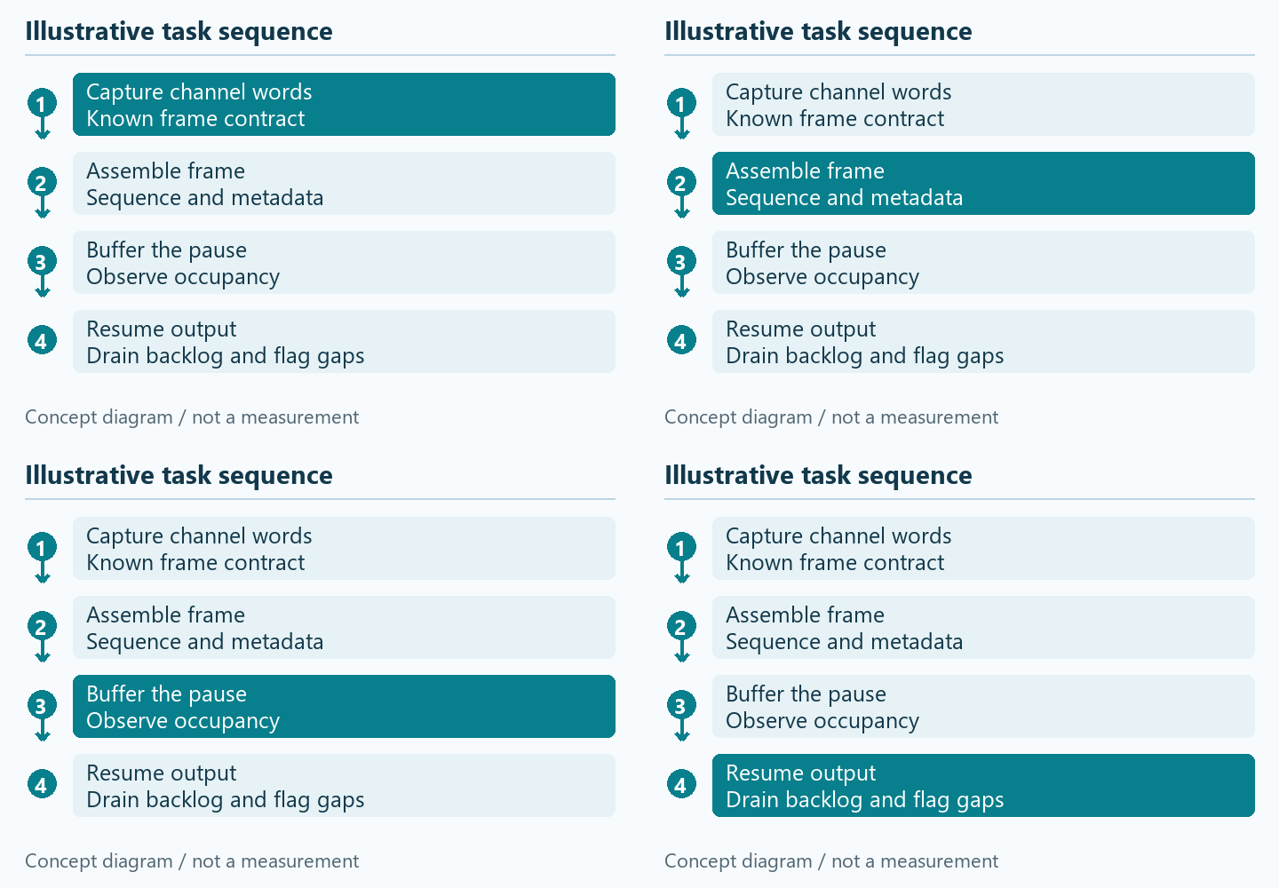
Sequence illustration and static alternative
Concept animation: highlighted stages show the order of checks, not elapsed time or a measured hardware result. Close the disclosure to hide motion. The numbered static diagram provides the same sequence.

Show the short illustrative animation
Continue the specific engineering task
- ad7606 — Review the exact device identity and linked documentation.
- XC7A100T 1CSG324C — Review the exact device identity and linked documentation.
- io budget — Use this related method or service to resolve the next requirement.
- bram budget — Use this related method or service to resolve the next requirement.
- resource budget — Use this related method or service to resolve the next requirement.
- Prepare an engineering review — Use this related method or service to resolve the next requirement.
Prepare an enquiry after reviewing the result
Copy or download your worksheet first. Include the exact part, quantity and unresolved conditions for a component enquiry, or board revision, requirements and test scope for a project discussion. These links open the enquiry entry; this page does not submit a request or promise automatic prefill.
Open the component enquiry entry · Discuss the engineering scope
Source scope and editorial method
Analog Devices AD7606 product and datasheet entry is the primary manufacturer reference for this article. Source check: 2026-11-13. This article presents planning methods; it does not establish measured prototype results, current stock or delivery availability.
Additional reference addresses (plain text; scope must be checked for the selected board and software):
ADI AXI AD7606X HDL reference — https://developer.analog.com/docs/hdl/library/axi_ad7606x/index.html