
Tutorials
FPGA Tri-State Bus Contention: Budget the Turnaround Between Drivers
Published · Updated
Give each driver an explicit ownership interval
A shared push-pull bus needs a rule for which device may drive it. Inactive output enable should release the pin; it should not merely drive the inactive data value. For an IOBUF, distinguish the data input, sampled input path and three-state control, and verify their polarity against the primitive documentation.

Draw both devices on the same time axis. Include reset and startup ownership, not only normal transfers. Two outputs driving the same value can hide an ownership bug until the data differs. A digital simulation that shows X during disagreement is useful evidence of a problem, but the absence of X does not prove safe electrical behavior.
Board bring-up sequence: Prepare the board checks before testing this interface.
I/O count and allocation: Reconcile signal count and physical allocation.
Compare the latest release with the earliest new drive
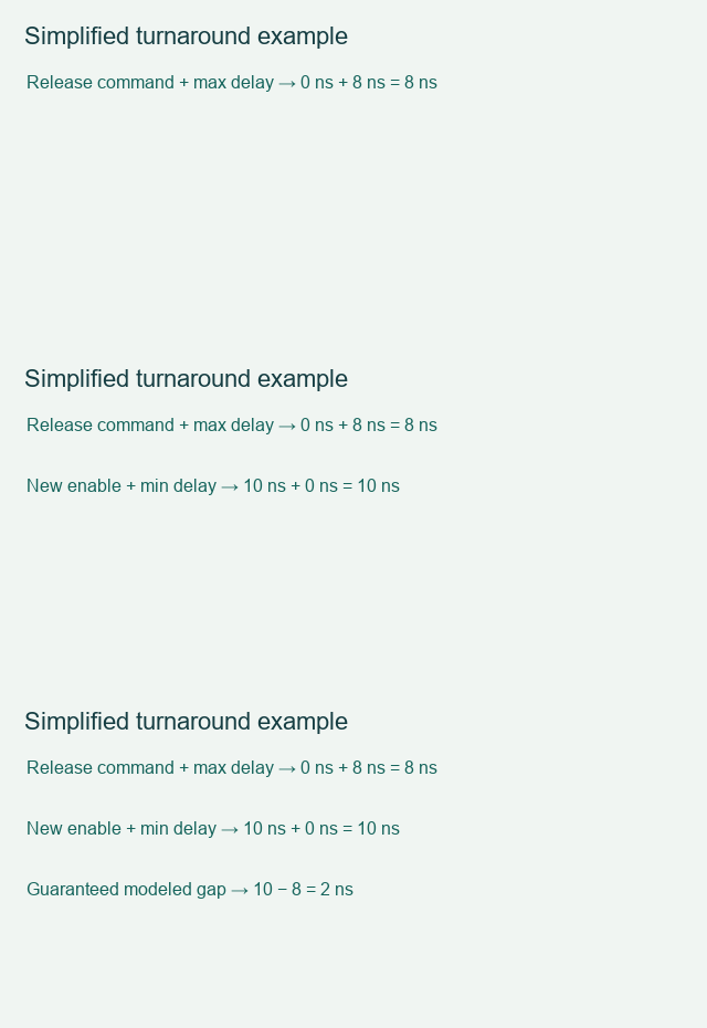
Suppose the old driver receives its release command at 0 ns and may take 8 ns to stop driving. If the next device receives enable at 10 ns and can begin driving immediately, the simplified guaranteed gap is 2 ns. Include the actual command timing, output-disable/enable limits, skew and uncertainty before applying that reasoning to a board.
The gap calculation is earliest new drive minus latest old release. A negative result indicates possible overlap under the entered bounds. A positive result alone does not establish a sufficient data-settling interval or valid receiver sampling time. It only addresses the ownership transition represented by the inputs.
External input/output timing: Include the external path in the timing budget.
Clock-domain synchronization: Keep asynchronous sampling separate from interface logic.
Check turnaround in both directions
Repeat the analysis for A-to-B and B-to-A. The two directions can have different delays and different controller behavior. Specify what the receiver samples during the undriven interval and whether a pull resistor or bus keeper is appropriate. Neither should be mistaken for another strong driver.
Save the waveform, enable-delay references and command relationship with the interface record. Review the implementation to ensure internal selection logic becomes the intended pin-level output-enable control. Then validate the external bus under representative conditions. Do not use a convenient one-cycle pause as proof until its real duration and the device delay bounds have been compared.
Power-on test record: Retain the power states and test sequence.
Use the equations and review steps above. Interactive checks require JavaScript.Watch the short simplified turnaround example sequence
Save the check result with your exact device, board revision and unresolved conditions. Discuss the interface requirements when the remaining issue needs a board or implementation review. Opening this link does not submit the worksheet.
Sources and example scope
Documentation checked 17 November 2026. Worked values are illustrative calculations. No board measurement or Vivado implementation run is claimed. The worksheet checks entered assumptions and does not inspect your schematic or project files.
Back to Tutorials