
Tutorials
FPGA Input and Output Delay Constraints: Build the External Timing Budget
Published · Updated
An FPGA can meet its internal timing and still violate the timing at a connected device. Input and output delays describe the part of the timing budget outside the FPGA. This worked example keeps the clock reference simple so that the signs and min/max values can be checked by hand.
Draw the clock reference before filling in numbers
Choose the edge and physical point that define time zero. The example below assumes a same-reference, single-data-rate interface with no external clock skew included. Both devices use the same ideal reference edge. Data-board delays are bounded; clock trace mismatch, jitter and uncertainty are not folded into those data delays.


A real board needs a more complete model when its clock arrives at different times at the two devices. Source-synchronous and DDR interfaces also require their own edge relationships. Stop and draw those relationships before adapting the example; do not add a convenient “margin” to every number and hope that the signs remain correct.
The probe photograph illustrates measurement access, not a measurement of this interface. A scope capture can help investigate timing, but probe loading, thresholds and measurement reference matter. Keep the source data sheet, receiver data sheet and board-delay estimate beside the budget. For a concrete acquisition context, see the AD7606 and Artix-7 throughput plan; its interface timing still requires the exact device data sheet.
Calculate both input-delay limits
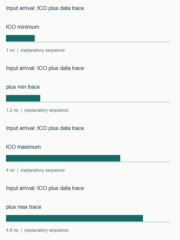
Assume that an external source changes its data 1.0–4.0 ns after the reference edge. The data trace contributes 0.2–0.8 ns. Under the stated zero-skew model, the earliest arrival at the FPGA pin is 1.2 ns and the latest is 4.8 ns. These are external arrivals, not delays through the FPGA input buffer.
set_input_delay -clock [get_clocks sys_clk] -min 1.2 [get_ports {din[*]}]
set_input_delay -clock [get_clocks sys_clk] -max 4.8 [get_ports {din[*]}]
Use the source device’s minimum and maximum clock-to-output specifications under the relevant conditions. A typical value is not a substitute for either bound. If the data sheet supplies no minimum, keep that as an unresolved input to the model instead of treating the maximum as both limits. The reference clock must exist before these constraints can refer to it.
Board propagation depends on the actual route and stackup. Use the trace-delay tool for an estimate with explicit assumptions, then replace it with the board analysis needed by the interface.
Keep the output hold sign visible
Now assume an external receiver needs 2.0 ns setup and 0.5 ns hold. With the same 0.2–0.8 ns data-board delay and zero external clock skew, the maximum output delay is 2.8 ns. The minimum is 0.2 − 0.5 = −0.3 ns. A negative minimum can be correct: the timing model still has to account for the receiver’s hold requirement.
set_output_delay -clock [get_clocks sys_clk] -min -0.3 [get_ports {dout[*]}]
set_output_delay -clock [get_clocks sys_clk] -max 2.8 [get_ports {dout[*]}]
Do not remove the minus sign to make the numbers look more intuitive. Instead, draw the earliest data change at the FPGA pin, add the fastest board delay, and compare it with the receiver’s hold boundary. That edge-by-edge check is more reliable than memorizing a sign without its reference.
| Quantity | Worked value |
|---|---|
| Input minimum / maximum | 1.2 ns / 4.8 ns |
| Output minimum / maximum | −0.3 ns / 2.8 ns |
| Unmodeled in this example | External clock skew, uncertainty, DDR edge selection and source-synchronous clock forwarding |
Check the model before exporting XDC
The calculator below uses only this model. It rejects reversed bounds and displays all four results together. Export the assumptions with the values; a bare set_output_delay line loses the receiver and board facts that justify it. Finally, inspect timing coverage and the actual input/output path reports. If the interface is constrained but fails, use path-level timing triage rather than widening the budget arbitrarily.
Same-reference SDR I/O budget
Inputs and exported records stay in this browser. The check evaluates the assumptions you enter; it does not inspect your project files.
Use the worked values and equations above, or download the examples below. The interactive check requires JavaScript.
Watch the short input arrival: tco plus data trace sequence
The sequence visualizes the stated example. It is not a hardware capture. The static figures and text above contain the same explanation.
Export the four bounds with their assumptions; include the source and receiver data-sheet tables in an interface review.
Download the timing and RTL examples (ZIP) · Discuss this engineering task
The ZIP includes the clock and I/O examples, timing-audit commands, counter/latch/reset RTL and testbenches. Bring the relevant exported record to the enquiry; this page does not submit it automatically.
References and example scope
Documentation checked 16 November 2026. AMD examples use the cited 2024.1 documentation baseline. Vivado commands and vendor macros were not executed for this article. Counter, latch and illustrative reset tests were executed with Icarus Verilog; latch structure was checked with Yosys. See the included commands and validation record for the exact scope.