
Tutorials
Artix-7 Programs over JTAG but Will Not Boot from Flash
Published · Updated
When an Artix-7 design runs after a JTAG download but disappears after power is removed, first establish which operation actually succeeded. Direct JTAG configuration loads the FPGA; it does not by itself create a persistent boot image in external memory. If flash programming and verification also succeeded, investigate the independent power-on configuration path before changing application logic. This guide provides an evidence-driven sequence and a copyable boot record. It describes troubleshooting methods, not measurements from a particular FPGA.io board.
Separate JTAG Configuration from Flash Boot
There are three useful paths to distinguish. A computer can configure the FPGA directly through a supported JTAG connection. A programming workflow can use the FPGA as a bridge to write supported attached configuration memory. After power is removed and restored, the FPGA must obtain its configuration through the board's selected boot arrangement. The second path prepares persistent contents; the third path proves whether those contents and the board configuration cooperate at startup.
A successful direct download therefore establishes only a limited result. The cable, programming software, target connection, and selected image were sufficient for that operation under those conditions. It does not establish the identity of the installed flash, the contents at the boot address, the mode-strap behavior, or the timing of power-on reset. It also does not establish that the same design will operate without a debugger, host command, or manually released reset.
Classify the symptom before touching settings. If flash has never been programmed, complete the documented persistent-programming workflow. If programming or verification fails, investigate that path first. If verification succeeds but independent startup fails, record the power-on configuration evidence. If configuration completes but the expected application behavior is absent, move to clock, reset, constraints, and software dependencies. These branches overlap, but keeping the first unproven stage visible prevents random changes.
Use the triage tool as an organizer, not a component-failure detector. Unknown is a valid answer. For example, an unobserved configuration-complete signal must not be converted into “configuration failed.” Record what you actually saw, how you observed it, and what remains unmeasured. That distinction matters when a remote engineer reviews the report without access to the board. The earliest verified boundary provides the strongest starting point for the next experiment.
Record the Exact Board and Tool Environment
Identify the full FPGA ordering code, board revision, installed configuration-memory part, schematic revision, and programming software version. Record the cable model and any adapter or onboard programming interface. The XC7A100T-1CSG324C device page is a contextual starting point for an Artix-7 example, not proof that the reader's package, memory wiring, or board constraints match it. Use the actual assembly record and device marking to resolve uncertainty.
Capture the intended configuration mode and how the board selects it. Identify relevant straps, jumpers, resistors, and any controller that can change a mode or reset condition. Record their state during direct programming and during independent startup. A test performed with a USB cable attached can differ electrically from a test powered only through the product's normal input. Describe all attached connections, including serial adapters that may unintentionally influence signals or power.
Make the programming file traceable to its source. Store the project revision, target part, build date, constraints revision, and a cryptographic hash of the image used. File names alone are weak evidence because an old file can be renamed or overwritten. Keep the flash image and the original FPGA image distinct in the record, together with the settings that produced the memory image.
Define one small observable application result suitable for the board. It might be a version register or a deliberately constrained indicator, but it must not rely on an undocumented external initialization step. Write the expected result before testing. If the design uses a processor or external memory, describe the additional software and initialization dependencies. A record that says only “LED off” cannot distinguish a failed configuration from a correctly configured design waiting for a clock, reset release, or software action.
Create and Verify the Configuration Memory Image
Use the programming instructions and supported configuration-memory list for the selected Vivado release. UG908's configuration-memory workflow distinguishes attaching the memory definition to the hardware target, preparing the image, and programming it. Follow the current documented procedure for the exact device and memory combination. This article intentionally does not provide a universal command with a guessed flash size, interface width, address, or memory identifier.
Check image generation settings against the board design. Record the intended boot address, memory interface, image format, and any configuration options that affect startup. Confirm that the memory image is generated from the same FPGA build that passed direct programming. If multiple images or fallback locations are used, retain the complete address map and the selection mechanism. Do not assume that programming a valid image at an arbitrary location makes it the boot image.
Review erase, program, and verify results separately. A progress bar reaching its end is not the same as a verification record. Save the tool log with the detected target, selected memory identity, image path and hash, address range, and final status. If verification fails, preserve the failure location and repeat only after checking the setup. Repeatedly erasing and rewriting without changing or observing anything adds wear and obscures the original failure.
Successful verification narrows the problem but does not prove independent boot. It supports a claim about the programmed contents under the verification method and conditions used. The FPGA must still select and read the intended memory path at startup. Before disconnecting the programmer, save the record and note whether the tool left a temporary configuration or reset state active. Then perform a separately defined power-cycle test, allowing the board's supplies and reset circuitry to reach the specified conditions rather than treating a software reconnect as a cold start.
Interactive planning worksheet
The worked method remains in the article. JavaScript adds input fields and a local summary export; no data is submitted.
Trace a Failed Power-On Configuration
Start with the board's approved power-up procedure and the configuration guidance in AMD UG470 for the applicable device and mode. Establish whether required rails and configuration-related signals reach their specified states. Use the schematic to identify actual measurement locations. This is not a generic pin-number recipe: package assignments, pull components, shared pins, and board-level logic must be checked against the chosen hardware.
Capture a sequence rather than isolated final values when timing may matter. A rail can read correctly after startup while having behaved incorrectly during configuration. Similarly, a mode signal observed long after reset may not reveal the value sampled at the relevant time. Define the event being observed, instrument settings, reference point, and trigger. Label conceptual diagrams as conceptual; only actual instrument captures should be presented as measured waveforms.
If the flash contents verified but configuration status is unknown, collect that status before blaming the image. If the configuration process reports an error, preserve the exact status and interpret it using the applicable documentation. Check that the expected memory is selected, that shared interface owners are released, and that the configured startup conditions match the board. Make one controlled change at a time and retain a baseline run for comparison.
Avoid making a board appear to pass by permanently leaving the programming cable connected. If that changes the result, it is evidence to investigate: compare power, ground reference, reset behavior, and any signals driven by the attached equipment. Record the difference without assuming its cause. A useful result can be a narrower question, such as “boot fails only when the host cable is absent.” That is a reproducible condition, whereas “flash unreliable” prematurely assigns the fault to a component.
Distinguish Configuration Completion from a Working Design
Treat configuration completion and application acceptance as separate observations. Once configuration has completed according to the applicable status interpretation, inspect the conditions needed by the user design. Is the expected clock present? Is reset released with the required sequencing? Are constraints bound to the correct board pins and I/O standards? Does the application require host commands, processor software, external memory initialization, or a peripheral-ready indication?
Compare the same design under direct JTAG configuration and independent boot. Keep the build hash, board connections, supply arrangement, and observation method fixed where possible. If the JTAG test automatically launches software or resets another device, document that extra action. The difference may be in the test procedure rather than in the stored FPGA image. An application that starts only after a debugger command is not yet an autonomous-startup demonstration.
Use a minimal diagnostic design only when its electrical behavior is appropriate for the board. Unconstrained or wrongly constrained outputs can create new problems. Identify a safe observation point and ensure the diagnostic design does not drive shared buses against another owner. If the diagnostic design boots and the full design does not, compare startup dependencies systematically instead of concluding that the larger image is inherently unsupported.
Retain application-level evidence that is hard to confuse with an old image. A version register or unmistakable build identifier is more useful than a generic blinking indicator reused in every build. Observe the result after removing the programming path and restarting the board normally. If configuration completes but application acceptance fails, preserve both facts. Reporting a single “boot failed” label would discard the distinction that should guide the next clock, reset, constraints, or software investigation.
Save a Reproducible Boot Test Record
Create a test matrix with separate rows for direct configuration, memory programming, memory verification, independent cold start, and application acceptance. Include the board and image identities on every run. Record the expected outcome, actual observation, connection arrangement, and the earliest failing stage. If a step was not performed, mark it not tested rather than borrowing the result from a different board or an earlier image.
Define what a cold-start test means for this design. State the power source, disconnection procedure, required discharge or reset conditions from the board specification, and attached equipment. Do not invent a universal waiting interval. If the device can be partly powered through an interface, account for that path. Test the intended customer arrangement as well as the laboratory arrangement so that a cable-dependent success is not mistaken for autonomous operation.
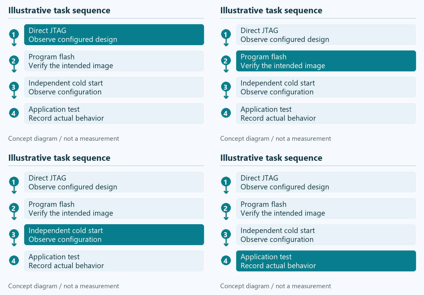
Use the interactive triage output to choose the next check and export the open evidence. Without JavaScript, apply the same sequence manually: establish direct configuration; establish supported flash identity and programming; establish verification; observe power-on configuration; then test application behavior. Stop at the first unknown or failed stage and gather evidence there. This is an ordering method, not a promise that every fault has exactly one cause.
When requesting assistance, provide the exact FPGA and memory identities, board revision, tool version, image hashes, relevant schematic excerpt, and the failing test row. Use the device page for a part-specific enquiry and the engineering entry for a board bring-up discussion. The article's copy and export controls do not send those materials automatically. Keep private design files out of public discussions unless you intend to share them, and distinguish a request for investigation from a claim that the board has passed engineering validation.
Sequence illustration and static alternative
Concept animation: highlighted stages show the order of checks, not elapsed time or a measured hardware result. Close the disclosure to hide motion. The numbered static diagram provides the same sequence.

Show the short illustrative animation
Continue the specific engineering task
- XC7A100T 1CSG324C — Review the exact device identity and linked documentation.
- vivado — Review this vendor-specific software workflow; support remains release-dependent.
- configuration storage — Use this related method or service to resolve the next requirement.
- fpga pcb bring up checklist — Use this related method or service to resolve the next requirement.
- power on plan — Use this related method or service to resolve the next requirement.
- Prepare an engineering review — Use this related method or service to resolve the next requirement.
Prepare an enquiry after reviewing the result
Copy or download your worksheet first. Include the exact part, quantity and unresolved conditions for a component enquiry, or board revision, requirements and test scope for a project discussion. These links open the enquiry entry; this page does not submit a request or promise automatic prefill.
Open the component enquiry entry · Discuss the engineering scope
Source scope and editorial method
Vivado UG908 — Programming Configuration Memory Devices is the primary manufacturer reference for this article. Source check: 2026-11-13. This article presents planning methods; it does not establish measured prototype results, current stock or delivery availability.
Additional reference addresses (plain text; scope must be checked for the selected board and software):
AMD 7 Series Configuration User Guide UG470 — https://docs.amd.com/v/u/en-US/ug470_7Series_Config