
Tutorials
Artix-7 Differential Pin Assignment: Match the Pair, Bank and Clock Route
Published · Updated
Match package pin names to the same differential pair
Two adjacent balls are not necessarily a differential pair. Use the pinout for the exact device and package. In the 7-series naming scheme, the pair identifier, P/N designation and bank number provide the relationship you need to check. A friendly schematic label such as DATA_P is only a net name; it does not prove that the assigned ball is the positive member of the intended pair.

Create one row per physical pair with both package balls, both device pin names, bank, direction and intended standard. Preserve the original pinout filename or revision. This makes a later package change visible instead of allowing old ball assignments to survive in a new schematic.
Board bring-up sequence: Prepare the board checks before testing this interface.
I/O count and allocation: Reconcile signal count and physical allocation.
Treat a clock input as a routing requirement
If the signal is a clock, verify clock-capable pin and routing requirements in addition to differential pairing. A general-purpose pair should not be assumed to provide the same clock resources as an appropriate clock-capable pair. Likewise, a pair that suits one clocking arrangement may not suit another region or resource connection.
Use the device tools to validate the proposed placement and inspect the resulting clock network. Keep electrical checks alongside the route check: common-mode range, differential amplitude, termination and bank supply. A correct P/N assignment cannot compensate for an incompatible source or receiver standard.
External input/output timing: Include the external path in the timing budget.
Clock-domain synchronization: Keep asynchronous sampling separate from interface logic.
Keep polarity, termination and constraints in one review
Trace each P and N net through connector numbering and any cable before finalizing constraints. Record an intentional polarity inversion explicitly; do not assume that every interface or primitive can absorb a swap. Confirm whether termination is external or internal and which conditions make it available.
The worksheet is a documentation completeness check. It does not manufacture legal package assignments. Export the record with the schematic and implementation report, then use the I/O timing article for the external arrival requirements. This keeps three separate approvals visible: correct physical pair, compatible electrical interface and supported timing/clock route.
Power-on test record: Retain the power states and test sequence.
Use the equations and review steps above. Interactive checks require JavaScript.Watch the short clock input review sequence
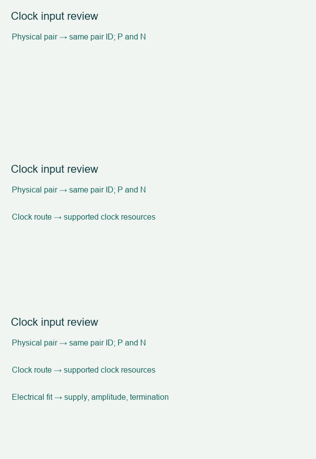
Save the check result with your exact device, board revision and unresolved conditions. Discuss the interface requirements when the remaining issue needs a board or implementation review. Opening this link does not submit the worksheet.
Sources and example scope
Documentation checked 17 November 2026. Worked values are illustrative calculations. No board measurement or Vivado implementation run is claimed. The worksheet checks entered assumptions and does not inspect your schematic or project files.
Back to Tutorials