
Tutorials
Artix-7 Flash Update Interrupted: Choose a Recovery Path
Published · Updated
After an interrupted Flash update, first establish what is still accessible. A working recovery image, an available external programming interface and preserved unique data lead to different next steps. Do not begin every recovery case with a full-chip erase.
Record what survived the interrupted update


Preserve the last programming log, selected image identity, target board revision and the point at which power or communication was lost. Record observations separately from assumptions: a disconnected client is not proof that the memory operation stopped at the same instant.
Use the board's documented power and connection procedure to inspect the current state. Record whether a recovery image actually responds and whether the expected target can be discovered through JTAG. Leave either result unknown until it has been observed.
Keep relevant configuration-status and pin observations with their capture time. Avoid mixing a current failure with a screenshot from a previous successful boot.
First separate flash boot from JTAG; a successful temporary load does not prove recovery.
If the symptom is intermittent, repeat the startup check under recorded conditions instead of accepting one successful cycle.
Choose a recovery image or external access
If the product's recovery image is confirmed to be running, follow that product's approved recovery procedure. If it is unavailable but the documented external programming route works, prepare the corresponding controlled reprogramming job. If neither path has been established, the next task is board-level access diagnosis rather than guessing a write command.
A recovery procedure published for an Alveo-based appliance can illustrate clear checkpoints without providing commands for an Artix-7 board. The same caution applies to automatic-update descriptions from other FPGA families. Identify the exact architecture before applying a procedure.
Do not treat successful JTAG discovery as permission to overwrite every memory region. It proves a useful access path, not the correct image or erase scope.
Preserve the failed attempt, then capture configuration status according to the board procedure.
Define what may be erased or replaced
Confirm the approved image, intended destination and regions that must survive. Calibration, unit identity and the recovery image may have separate preservation requirements. Record whether a reliable backup exists and whether the board's procedure permits reading or restoring that information.
Review the actual erase granularity and programmer range. Byte-separated images can share an erase unit. A recovery operation that restores the application but destroys required per-unit data is not a successful product recovery.
If image protection or access restrictions affect the procedure, use the approved product-specific path. Do not add generic security-reset or provisioning commands to a recovery checklist.
To narrow the startup phase, observe configuration pins and timestamp the observation.
Verify through an independent boot
After the permitted rewrite and its required verification, perform the specified independent startup procedure. Obtain a fresh running-build observation where the design supports it and execute the required application checks. A temporary design loaded over JTAG does not establish persistent recovery.
Keep the interrupted attempt and recovery attempt as separate records. Note which image was restored, which regions changed and which acceptance tests were actually completed. Preserve unresolved checks rather than collapsing everything into a single restored label.
The recovery worksheet exports the current evidence, candidate path and stopping conditions. It does not connect to hardware or promise that a board is repairable. Use the report, exact board identity and sanitized log when requesting engineering assistance.
| Evidence obtained | What remains unresolved |
|---|---|
| Expected FPGA appears over JTAG | Stored image and persistent boot |
| Temporary JTAG design runs | Flash contents and independent startup |
| Memory verification completes | Boot selection, startup and application behavior |
| Independent boot reaches expected build | Any application tests still required by the product |
After a permitted rewrite, confirm the recovered build from the actual running design.
Technical references for this scope: AMD UG470 v1.17 (2023-12-05); AMD UG908 2024.1 — Programming a Configuration Memory Device.
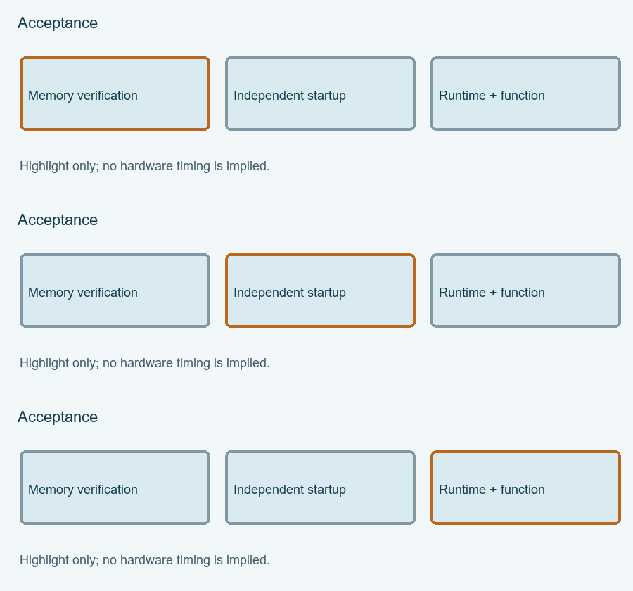
Highlight the three review items
Each highlight marks one item to review, not elapsed hardware time. The static figure contains the same information.
Enable JavaScript for the local Interrupted-update recovery triage. The article above provides the manual procedure; no data is submitted automatically.
Review and export your result before opening the engineering discussion entry. Attach the exported text yourself; opening the entry does not submit it.
Reference scope checked 15 November 2026. Calculations and conceptual diagrams describe the stated model. Commands and board behavior require validation in the actual tool and board environment.