
Tutorials
Artix-7 Configuration Flash Size: Budget One or Two Images
Published · Updated
A Flash that holds the first FPGA image may still be too small for the product. A second image, reserved data and alignment can change the answer. Start with a storage budget that describes those requirements, then separately establish whether the chosen Flash works with the board and configuration flow.
For the 7A100T, UG470 v1.17, Table 1-1 lists a configuration bitstream length of 30,606,304 bits and a minimum configuration Flash size of 32 Mb. Treat this as the manufacturer's device baseline. It is not a guarantee that every production package, multiple-image layout or future release fits the same minimum.
Start with the device and the actual image

Keep the FPGA ordering code and board revision beside the image record. The XC7A100T-1CSG324C device page identifies one ordering variant; a photograph of another package does not establish its pinout or board compatibility. Capacity planning does not remove the need to check those details.
Divide the baseline bit count by eight to express it in bytes: 30,606,304 / 8 = 3,825,788 bytes. This conversion is arithmetic, not a measurement of a generated file. For a real layout, determine the occupied memory range from the actual output and generation settings. In particular, the number of bytes occupied by an MCS text file on a computer is not the number of Flash bytes its address records describe.
Keep a current value and a release allowance. A measured current image answers what this build occupies. An allowance answers how much space the product reserves for later builds. If the project cannot establish a maximum, record that uncertainty rather than silently assuming the current file will never grow.
Compression can be useful, but one compressed output is not a bound on every future output. If a reduced image size drives a component decision, the release process must identify how later builds are checked against the allocation. Otherwise, a software update can create a hardware storage problem after the board has been committed.
Allocate slots, alignment and reserved data
For an initial budget without fixed start addresses, define each image allowance L_i in bytes, a slot alignment A in bytes, and a separate reserved allocation R. The rounded slot is ceil(L_i / A) × A. Sum the rounded slots and add R. This model estimates an allocation; it does not select a valid boot address or prove that an erase operation preserves nearby data.
Consider a deliberately specified calculation: two image allowances of 3,825,788 bytes each, 65,536-byte slot alignment, and 1 MiB reserved outside the slots. Each rounded slot is 3,866,624 bytes. Two slots plus the reserve require 8,781,824 bytes. An 8 MiB memory contains 8,388,608 bytes, so this plan is short by 393,216 bytes.
The alignment in this example is an input, not a statement about every Flash's erase geometry. The reserved allocation is also a project assumption. Replace both with justified values before using the result. A useful calculator should display those assumptions next to the answer, not conceal them behind a suggested part number.
Fixed addresses require another check. Two images may fit in total capacity but occupy overlapping ranges. They can also occupy different byte ranges while sharing an erase unit. Review both data occupancy and the actual erase operation when constructing the address map. A simple total-capacity calculation cannot settle either question.
The configuration storage tool is the existing place to start the budget. Record which quantities it includes and add any omitted allocation explicitly. Do not add the same reserve both inside each image allowance and again as a separate region.
Separate enough space from supported hardware
After the arithmetic passes, the engineering work is not finished. Check the complete Flash ordering code, supply and interface requirements, board connections, boot mode and support in the programming flow. A density label is not a substitute for those checks. A larger memory is not automatically a drop-in replacement.
The W25Q128JVSAQ catalogue entry can be used as a candidate record when investigating a design. Its presence in this article is not a compatibility recommendation for the stated FPGA or for every SPI mode. Establish compatibility from the exact device documentation, board circuit and supported tool configuration.
Keep the tool's capacity unit visible. AMD's configuration-memory generation guidance distinguishes the byte-based size argument from the bit-based density commonly used for Flash. Normalize units before entering parameters. Do not copy a density number straight into a command simply because both fields say size.
When a generated image fits and programs successfully, verify the independent boot path. The Artix-7 flash-boot checks cover that separate stage. A capacity result should never be presented as evidence that the FPGA has started from the intended image.
Save the assumptions for the next release
A useful budget survives beyond today's component choice. Save the device and board revision, generated-image identity, allowance per image, slot alignment, reserved regions, memory capacity and date. Distinguish measured values from proposed allowances. Keep the source of each input so that a later engineer can update the calculation without guessing why a margin exists.
For every release, compare the new image's occupied range with its allowed region before programming a board. If an allocation changes, review the rest of the map and the update/recovery process. Increasing one slot can affect another image or data that the update must preserve.
The output should contain two conclusions. First, does the stated allocation fit the entered capacity? Second, which compatibility and boot checks remain unresolved? A result can correctly say “capacity sufficient” while leaving hardware support unconfirmed. That is more useful than an overall green badge.
Save the budget with the release package. For a component or board review, open the engineering review entry and attach the budget, intended Flash ordering code and unresolved checks. The reviewer then has a concrete allocation to evaluate rather than a question about whether a chip is simply large enough.
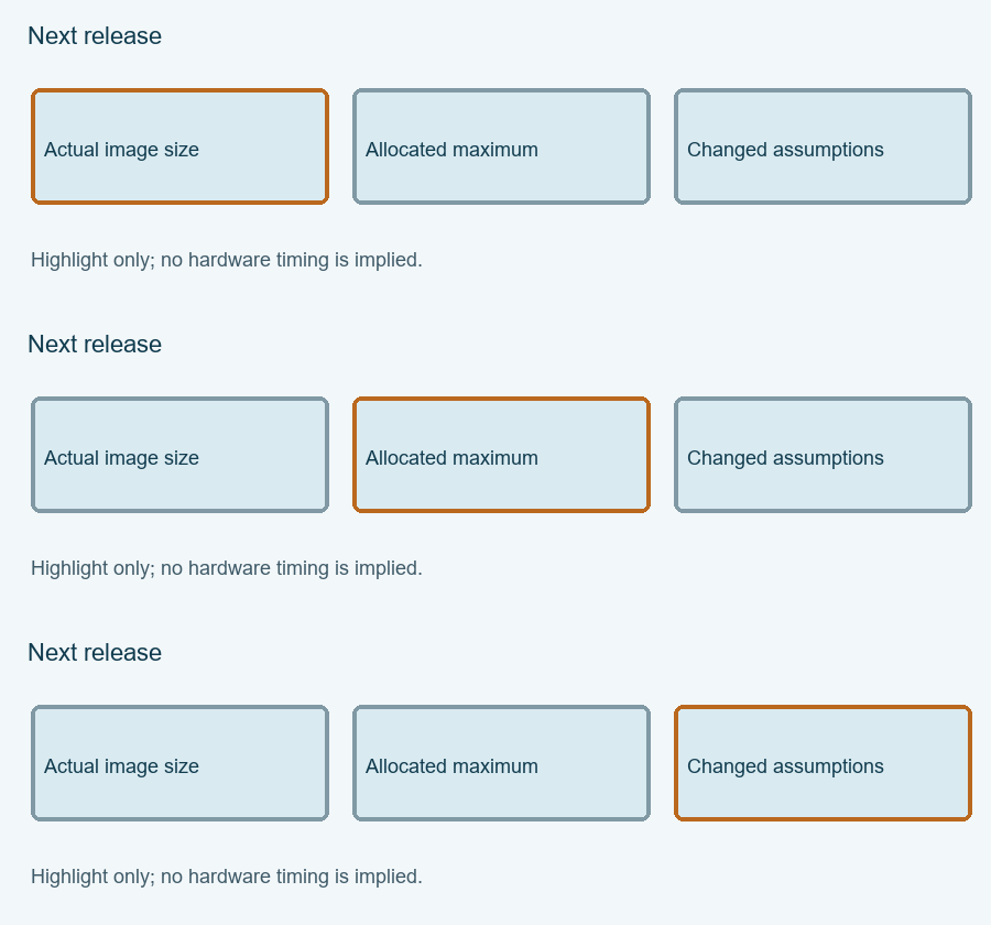
Highlight the three review items
Each highlight marks one item to review, not elapsed hardware time. The static figure contains the same information.
Enable JavaScript for the local Image-slot capacity budget. The article above provides the manual procedure; no data is submitted automatically.
Reference scope checked 15 November 2026. Calculations and conceptual diagrams describe the stated model. Commands and board behavior require validation in the actual tool and board environment.