
Tutorials
Artix-7 I/O Bank Voltage Planning: Check the Rail Before Assigning Pins
Published · Updated
Start with the bank rail, not the connector pin
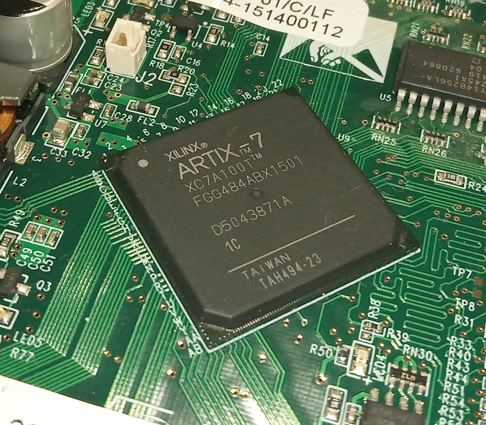
A connector can have enough free pins and still be unusable for an interface. Before assigning a package ball, write down the complete FPGA ordering code, package, board revision and supply connected to each bank. Then add signal direction and the intended I/O standard. The shared bank supply is a board connection; changing an XDC property does not change that voltage.

Keep input and output requirements separate. A standard that can be received under a particular set of conditions does not automatically permit an output using the same bank supply. Reference-voltage and termination requirements also belong in the record. An empty VREF cell should mean “not checked” until the chosen standard establishes whether it is needed.
Board bring-up sequence: Use the board bring-up sequence to place this rail check before external connections.
I/O count and allocation: The I/O budget estimates pin demand; add the bank-compatibility record before allocating those pins.
Find conflicting requirements before routing
Consider two proposed outputs in one bank: one interface requires a 3.3 V bank supply and the other requires a 1.8 V bank supply. Labeling their pins LVCMOS33 and LVCMOS18 cannot satisfy both requirements. Moving one interface to a suitable bank, changing the interface architecture, or adding an appropriate translator are design choices; suppressing a tool warning is not a voltage conversion.
The worksheet below checks whether the rail requirements you entered conflict. It deliberately does not contain a device database. Matching numbers only show that your entries are consistent. They do not establish support for the standard, adequate drive strength, legal reference pins or a valid clock route. Retain the original pinout and standard table with the result.
External input/output timing: Once electrical compatibility is established, record the external input/output timing.
Clock-domain synchronization: An asynchronous control input needs its own synchronization analysis.
Reconcile the schematic, pin plan and implemented design
Export the implemented I/O report and compare it against the schematic net list. Check package ball, bank, signal direction and I/O standard for each external signal. Pay particular attention to spare pins that were reassigned late in layout. A correct interface description attached to the wrong package ball remains a board error.
Before board release, record who owns each unresolved row and what evidence will close it: a revised schematic, a package pinout entry or a tool report. At bring-up, measure the actual bank rail before connecting an external driver. This workflow separates an intended voltage from a measured one and prevents a convenient spreadsheet default from becoming a hardware assumption.
Power-on test record: Keep actual rail measurements in a power-on test record.
Use the equations and review steps above. Interactive checks require JavaScript.Watch the short output requirements in one bank sequence
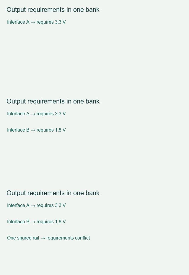
Save the check result with your exact device, board revision and unresolved conditions. Discuss the interface requirements when the remaining issue needs a board or implementation review. Opening this link does not submit the worksheet.
Sources and example scope
Documentation checked 17 November 2026. Worked values are illustrative calculations. No board measurement or Vivado implementation run is claimed. The worksheet checks entered assumptions and does not inspect your schematic or project files.
Back to Tutorials