
Tutorials
Artix-7 Pins Before Configuration: Plan External Enables and Pull Resistors
Published · Updated
Define the external state before the RTL starts
An output assignment in RTL does not control the entire power-up interval. Before configuration and startup complete, external enables, chip selects and reset nets need an intentional board-level state. Begin with the receiving device: what happens if the net is high, low or floating at each stage?
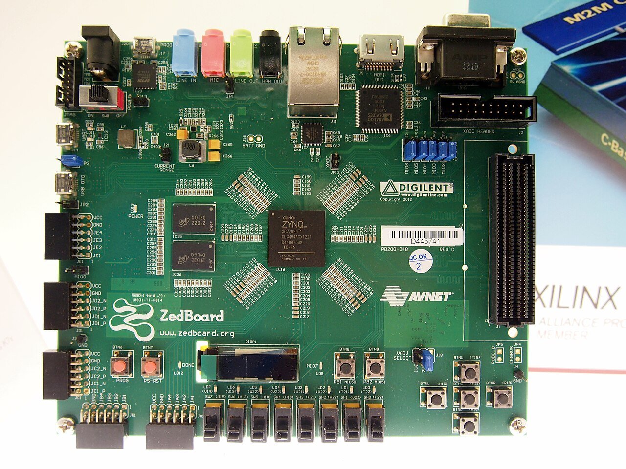

Make a phase table for power absent, rails rising, configuration, startup, normal operation and reconfiguration. Record the active driver and pull resistor in each row. Include the external device supply, because a high level from an already powered peripheral can reach an FPGA whose bank is not yet powered.
Board bring-up sequence: Prepare the board checks before testing this interface.
I/O count and allocation: Reconcile signal count and physical allocation.
Use PUDC_B with its documented scope
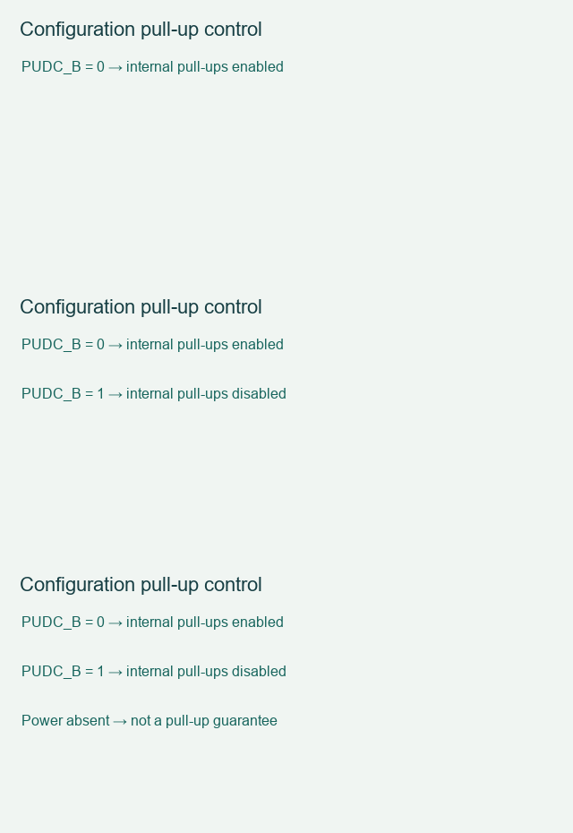
UG470 describes PUDC_B as the control for internal SelectIO pull-ups during configuration: low enables them and high disables them. This is a configuration behavior, not a general promise that every external control net has its desired state throughout every power condition. Power sequencing and multifunction pins require their own checks.
Do not substitute an RTL PULLUP setting for the configuration-time analysis. Follow the PUDC_B connection requirements in the configuration guide and examine the dedicated or multifunction role of each affected pin. For an external enable whose default is important, evaluate an explicit board-level bias and the receiving device thresholds rather than relying on an unspecified floating state.
External input/output timing: Include the external path in the timing budget.
Clock-domain synchronization: Keep asynchronous sampling separate from interface logic.
Capture the handover to user logic
Review the instant when control transfers from configuration behavior to user logic. A peripheral may react to a short pulse even if the final state looks correct. Keep output enables inactive until the relevant clock and reset sequence establishes a valid operating state.
The phase worksheet below highlights missing ownership; it cannot measure a startup glitch. At board validation, capture the relevant rail, configuration indicator and external control net with a suitable measurement setup. Repeat cold start and reconfiguration separately. Record probe reference and trigger condition so the trace can be interpreted, and do not treat a successful warm restart as proof of cold-start behavior.
Power-on test record: Retain the power states and test sequence.
Use the equations and review steps above. Interactive checks require JavaScript.Watch the short configuration pull-up control sequence
Save the check result with your exact device, board revision and unresolved conditions. Discuss the interface requirements when the remaining issue needs a board or implementation review. Opening this link does not submit the worksheet.
Sources and example scope
Documentation checked 17 November 2026. Worked values are illustrative calculations. No board measurement or Vivado implementation run is claimed. The worksheet checks entered assumptions and does not inspect your schematic or project files.
Back to Tutorials