
Tutorials
FPGA Button Debounce: Separate Synchronization, Stability and the Press Pulse
Published · Updated
Synchronize the input before qualifying a press
A mechanical button can produce several transitions during one action. It is also asynchronous to the FPGA clock. These are separate problems: synchronization reduces the risk associated with sampling an asynchronous signal, while debouncing decides when a new mechanical state has persisted long enough. A long counter alone is not a substitute for the synchronization structure.
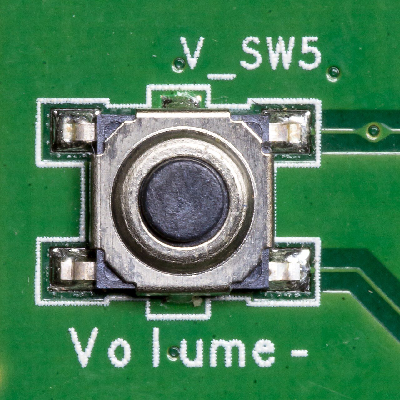

Keep three signals visible in the design: synchronized sample, debounced state and one-cycle press event. This avoids using a held button as a repeated command. Decide whether the application needs release events, long-press behavior or only a single action on the inactive-to-active transition.
Board bring-up sequence: Prepare the board checks before testing this interface.
I/O count and allocation: Reconcile signal count and physical allocation.
Define exactly what N stable samples means
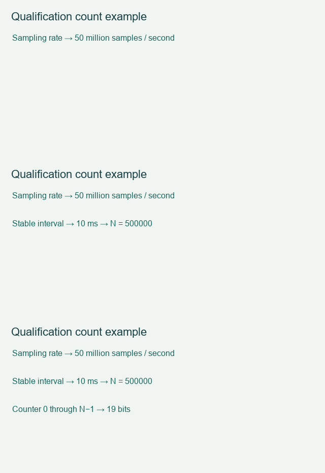
One useful contract accepts a new state after N consecutive samples of that state, resetting the candidate count whenever the sample changes back. Derive N=ceil(clock frequency×qualification time) for a counter evaluated every clock. At 50 MHz and 10 ms, N is 500000; a counter representing zero through N−1 needs 19 bits.
If the design samples only on a slower enable, use that sampling rate instead. Define the N=1 case explicitly. The qualification interval is a design choice informed by the actual switch and required response, not a universal maximum bounce duration. Apply the same reasoning to release unless the application intentionally specifies otherwise.
External input/output timing: Include the external path in the timing budget.
Clock-domain synchronization: Keep asynchronous sampling separate from interface logic.
Test the boundary and the held-button behavior
Construct test sequences with N−1, N and N+1 consecutive samples, an interrupted candidate sequence, a long hold and release bounce. Count emitted press pulses rather than merely looking at the final state. Reset during a candidate transition should have an intentional result.
The timing worksheet below calculates the interval and counter width; it does not claim a hardware measurement. For RTL verification, make the expected event sequence independent of the implementation counter. On a real board, capture both the raw input and the debounced event where possible. This makes it clear whether a failure comes from switch behavior, synchronization, qualification or downstream event handling.
Power-on test record: Retain the power states and test sequence.
Use the equations and review steps above. Interactive checks require JavaScript.Watch the short qualification count example sequence
Save the check result with your exact device, board revision and unresolved conditions. Discuss the interface requirements when the remaining issue needs a board or implementation review. Opening this link does not submit the worksheet.
Sources and example scope
Documentation checked 17 November 2026. Worked values are illustrative calculations. No board measurement or Vivado implementation run is claimed. The worksheet checks entered assumptions and does not inspect your schematic or project files.
Back to Tutorials