
Tutorials
FPGA GPIO LED Resistors: Check the Current at Both Voltage Corners
Published · Updated
Identify whether the FPGA sources or sinks the LED current
Trace the current path on the actual schematic. In a source arrangement, the FPGA output supplies current through the LED and resistor toward ground. In a sink arrangement, the supply feeds the LED and resistor and the FPGA pulls the return low. The active logic level and relevant output-voltage specification differ.


The Basys 3 rev. C reference manual describes user LEDs connected through 330 ohm resistors and illuminated by a high output. That is a fact about that board, not a universal FPGA resistor recommendation. Board photographs help locate components; the schematic establishes their electrical connection.
Board bring-up sequence: Prepare the board checks before testing this interface.
I/O count and allocation: Reconcile signal count and physical allocation.
Use voltage and resistance corners
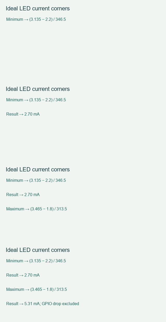
For an initial ideal-source estimate, I=(V−Vf)/R. Maximum current uses the largest applied voltage, smallest LED forward voltage and smallest resistor value. With 3.3 V ±5%, Vf from 1.8 to 2.2 V and a 330 ohm ±5% resistor, the estimate spans about 2.70 to 5.31 mA. This deliberately simple calculation does not model GPIO voltage droop.
Check guaranteed VOH or VOL at the intended current, the selected I/O standard, drive setting and applicable device limits. Also check LED current and resistor power. A drive-strength attribute is not an ideal constant-current source. Several simultaneously lit LEDs add load and switching activity to the bank and supply system.
External input/output timing: Include the external path in the timing budget.
Clock-domain synchronization: Keep asynchronous sampling separate from interface logic.
Validate brightness and power with the actual circuit
Use the calculation to identify a sensible evaluation range, then inspect the real output voltage and current. Include temperature and assembly variants when they matter. If the required current cannot be supported with adequate logic levels and device margin, evaluate an external driver instead of increasing the FPGA drive setting blindly.
For multiplexed or PWM LEDs, distinguish peak current from average current and verify pulse conditions against the LED and driver specifications. The calculator below estimates continuous current corners. It does not approve a pulsed overcurrent condition or determine perceived brightness. Save the direction, device limits and chosen resistor with the BOM review.
Power-on test record: Retain the power states and test sequence.
Use the equations and review steps above. Interactive checks require JavaScript.Watch the short ideal led current corners sequence
Save the check result with your exact device, board revision and unresolved conditions. Discuss the interface requirements when the remaining issue needs a board or implementation review. Opening this link does not submit the worksheet.
Sources and example scope
Documentation checked 17 November 2026. Worked values are illustrative calculations. No board measurement or Vivado implementation run is claimed. The worksheet checks entered assumptions and does not inspect your schematic or project files.
Back to Tutorials