
Tutorials
FPGA BRAM Utilization: Why Enough Bits Can Still Require More Blocks
Published · Updated
Start with the port organization, not the bit total
A 20-bit-wide memory with 1,024 addresses needs 20,480 payload bits. Dividing that number by a primitive capacity gives a useful lower bound, but it does not tell you how many physical blocks the tools will allocate. Port count, supported widths, byte enables and clocking can prevent a seemingly compact arrangement.
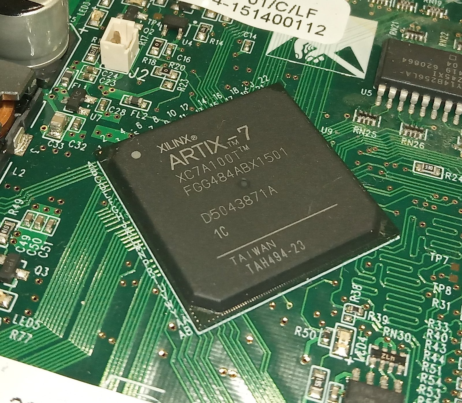

Write the required width and depth before selecting a primitive mode. For 7-series devices, RAMB18E1 and RAMB36E1 have specific configurations; the widest simple-dual-port arrangement is not interchangeable with a true-dual-port arrangement. Parity positions, ECC and output registers add further conditions. Keep the selected mode with your calculation instead of treating every bit in the device as freely interchangeable storage.
Estimate other resource requirements.
Place the memory estimate within the acquisition budget.
Compare two ways to tile the same memory
Suppose the permitted tile in your design is 1,024 words by 18 bits. A 1,024-by-20 request needs two tiles side by side: two extra bits in each word force a second width slice. The allocated capacity is 36,864 bits, while payload is 20,480 bits, giving 55.56% payload utilization. This is an arithmetic example using the stated tile, not a synthesis result.
The worksheet uses ceil(requested width / tile width) multiplied by ceil(requested depth / tile depth). Try a different supported tile and compare the arrangement. Do not enter a convenient but illegal tile. Also distinguish allocated capacity from power or throughput: unused positions do not translate directly into a measured power saving.
Use the BRAM organization worksheet.
Close the estimate against the implemented memory
Inspect the inferred primitives, their modes, the resulting address decode and the read latency. A large register array may have failed to infer BRAM because its read behavior or reset behavior cannot map to the intended primitive. Changing a capacity estimate will not fix that coding mismatch.
Retain the RTL revision, exact device, synthesis version, inferred memory count and warnings in one record. The downloadable organization record is a planning aid; this article supplies no fabricated Vivado report. If the tool count differs, investigate port behavior and mode selection before concluding that the FPGA resource table is wrong.
Keep the exact device and package.
Width boundary: 1024-word depth: short sequence
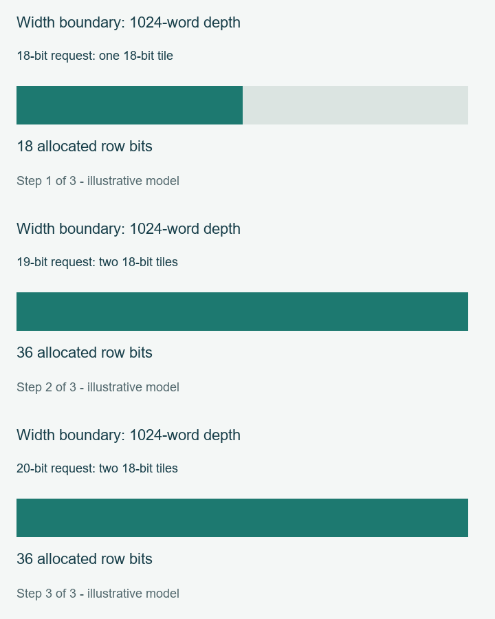
18-bit request: one 18-bit tile: 18 allocated row bits → 19-bit request: two 18-bit tiles: 36 allocated row bits → 20-bit request: two 18-bit tiles: 36 allocated row bits
Export your result with its assumptions. For an unresolved board or implementation issue, prepare an engineering review with the exact part, revision and relevant record. This link opens the review page; it does not send your worksheet.
Sources and scope
Sources checked 18 November 2026. Numerical examples are calculated cases. Hardware measurements and device timing closure are outside the results shown here.
Back to Tutorials