
Confirmed here
The source-listed identity XC3SD3400A-5CSG484C and 0 individually sourced technical fields shown below.
Open identity evidence ↓AMD / Xilinx / TECHNICAL REFERENCE
A documented ordering-code reference associated with XC3SD3400A. Literal distributor listing, retained as identity evidence only; no availability or technical-specification claim.
FPGA.io Part Number FIO-3C89D929A1329971Internal catalogue reference · manufacturer MPN remains unchanged
Technical reference · Documented ordering reference · Checked 2026-09-28
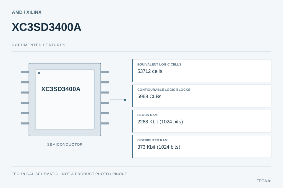
The source-listed identity XC3SD3400A-5CSG484C and 0 individually sourced technical fields shown below.
Open identity evidence ↓Use XC3SD3400A resources to understand the silicon. They do not establish the I/O count or electrical limits of every package.
Read base-device parameters →Any package, speed, temperature, lifecycle or electrical field absent from the sourced table needs confirmation. Stock, price and delivery also require a current quotation.
Request exact-code review →DOCUMENTED FACTS
This reference establishes the published ordering identity. Package-specific electrical and timing parameters have not been reviewed here. Use the base-device documentation as context, then verify the exact package and grade.
| Parameter | Documented value | Source & conditions |
|---|---|---|
| Manufacturer part number | XC3SD3400A-5CSG484C | Published identity ↗Product title and manufacturer part number |
This ordering reference contains the documented facts shown above; it is separate from the fully reviewed FPGA ordering-number catalogue.
Include the full ordering code, quantity, delivery requirement and traceability needs. For an assembled board, include BOM revision, programming and test scope.
Request this device ↗Compare the documented requirements; inclusion in the same series does not establish interchangeability.
BASE DEVICE
Spartan-II base device for legacy design maintenance. Package, speed and temperature suffixes are required to identify an orderable part.
BASE DEVICE
Spartan-IIE base device for legacy design maintenance. Package, speed and temperature suffixes are required to identify an orderable part.
BASE DEVICE
Spartan-3 base device for legacy design maintenance. Package, speed and temperature suffixes are required to identify an orderable part.
BASE DEVICE
Spartan-3A base device for legacy design maintenance. Package, speed and temperature suffixes are required to identify an orderable part.