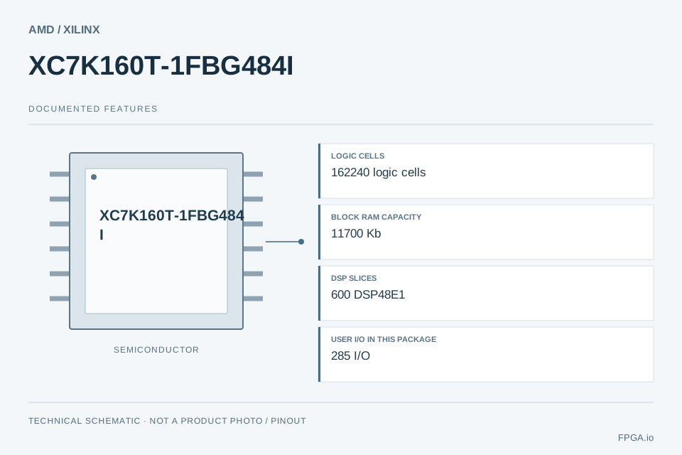
- Logic cells
- 162240 logic cells
- Block RAM capacity
- 11700 Kb
- DSP slices
- 600 DSP48E1
- User I/O in this package
- 285 I/O
No verified supplier stock or price is currently displayed here. Request a quotation for your quantity and required delivery date.
Supplier references are independent of FPGA.io inventory. Confirm currency, region, quantity tier, packing, taxes, freight and final terms at source.
Check this exact MPN at external distributors
Search links do not establish stock, price or an authorized distribution relationship. Check the full code, package and grade at the source.
Already have a target price or delivery date? Request a Better Quote ↗
PRODUCT OVERVIEW
About XC7K160T-1FBG484I
XC7K160T-1FBG484I is an FPGA in the AMD / Xilinx Kintex-7 family, supplied in the FBG484 package. Its reviewed resources include 162,240 logic cells, 11,700 Kb of block RAM, 285 I/O for this device/package combination. This ordering code specifies speed grade -1 and Industrial (I) temperature grade. The selected device/package has 4 GTX channels; check this package-level limit before planning serial interfaces. Use the linked manufacturer data sheets for electrical limits, pin assignments and timing. FPGA.io can review the complete part number for chip sourcing or a combined sourcing and PCBA project.
- Logic cells162,240 logic cells
- Block RAM capacity11,700 Kb
- DSP slices600 DSP48E1
- User I/O in this package285 I/O
- Package codeFBG484
- Junction temperature (Tj)-40 to +100 °C
Review parameter sources and conditions ↓Technical specifications
Core device, package and grade fields are linked to official documents. The full MPN is evidenced by a historical manufacturer listing; current lifecycle and availability require confirmation. Voltage, application timing and power are not fully characterized here.
Logic & memory
Package & interfaces
Operating conditions
Supply & status
MANUFACTURER REFERENCES
Official documents & PDF datasheets
Use the electrical data sheet together with the device overview and package/pinout information.
Primary data sheetDS182 — Kintex-7 DC and AC Switching CharacteristicsElectrical operating conditions and speed-grade timing tables; select the applicable grade. · Rev 2.19 · 2021-03-26Official PDF ↗Data sheet / device reference7 Series FPGAs Data Sheet: Overviewpp. 2-4, Tables 2-7; p. 7 CLBs, Slices, and LUTs; p. 16 Figures 1-2 · Rev 2.6.1 · 2020-09-08Official manufacturer documentation ↗Data sheet / device referenceKintex-7 FPGAs Data Sheet: DC and AC Switching Characteristicsp. 3, Table 2, Temperature; p. 1 introduction; p. 41 Table 35 DSP48E1 · Rev 2.19 · 2021-03-26Official manufacturer documentation ↗Package & pinout7 Series FPGAs Packaging and Pinout Product Specificationpp. 10-18 package/transceiver/I/O tables; pp. 255-291 mechanical drawings · Rev 1.20 · 2024-03-13Official manufacturer documentation ↗Package & pinoutProduct Discontinuation Notice for Selective FFV, FBV and SBV Device PackagesTable 4, page 2; Table 5, pages 3-4; Replacement Part columns only · Rev 1.0 · 2020-09-28Official PDF ↗Full ordering-number evidence: XCN20011 v1.0, p. 3, Table 5, left table block, data row 2, Replacement Part column.
Manufacturer documents may be revised. Verify the current revision and applicable device/package/grade before releasing a design.
ENGINEERING SELECTION
What these specifications mean for your design
Use the documented resources of XC7K160T-1FBG484I to frame a design review. The guidance below interprets the source data; it does not establish achieved system performance.
Logic implementation
162,240 logic cells
Use this native resource count for an initial budget. LUT, logic-cell and logic-element definitions differ; synthesize your HDL in the target toolchain to establish fit and timing.
Manufacturer evidence ↗ Conditions ↓Buffers and local storage
11,700 Kb
Budget sample buffers, FIFOs and coefficient storage in bits, then check memory block geometry, port widths, clocking and reserved capacity. External memory needs a separate interface review.
Manufacturer evidence ↗ Conditions ↓Arithmetic and signal processing
600 DSP48E1
Map the required multiply/accumulate operations, operand widths and pipeline stages to the documented DSP architecture. A resource count does not establish throughput.
Manufacturer evidence ↗ Conditions ↓Board connections
285 I/O
This count applies to the selected device/package. Budget required signals and spare capacity, then check bank voltages, differential pairs, dedicated pins and configuration use in the pinout guide.
Manufacturer evidence ↗ Conditions ↓High-speed serial planning
4 GTX
Channel count is only a starting point. Confirm lane availability, reference clocks, electrical limits, line rate, protocol IP and licensing for the exact device/package and speed grade.
Manufacturer evidence ↗ Conditions ↓PCB and assembly planning
FBG484
Check the official footprint, pin/ball map, pitch, escape routing, power/ground distribution and assembly constraints. Package name or ball count alone does not prove pin compatibility.
Manufacturer evidence ↗ Conditions ↓Operating environment
-40 to +100 °C
Check whether this range is specified at junction or ambient, together with the source conditions. Estimate power and cooling for your design before selecting the temperature grade.
Manufacturer evidence ↗ Conditions ↓Application paths to evaluate
These are engineering evaluation directions based on documented resources, not verified reference designs or application certifications.
Control and interface logic
Evaluate state machines, parallel interfaces and I/O expansion against the documented I/O budget, bank standards and timing. Select external level shifting or interface devices where required.
Build a resource budget →Buffered signal processing
Evaluate filters, sample buffering and pipelined arithmetic using the documented DSP and block RAM resources. Validate precision, memory bandwidth, clock closure and application power in the actual implementation.
Build a resource budget →Serial-link designs
Evaluate a lane and clock budget using the documented channels. Protocol support, achievable line rate and IP availability must be confirmed separately; channel count alone does not qualify an interface.
Build a resource budget →Achievable clock frequency, power consumption and interface performance depend on the implemented design, operating conditions and timing closure. Use the applicable electrical data sheet and vendor analysis tools.
Before placing this part on a board
- Use the full ordering number. Check the package pinout, power banks, speed grade and temperature range together.
- Complete timing and power analysis. A resource table cannot predict achievable frequency or application power.
- Define the manufacturing scope. Share the BGA footprint, stack-up, assembly requirements and test plan with your PCBA request.
Plan assembly for your FPGA board →
FROM SELECTION TO A BOARD
Design resources & implementation options
When to evaluate another implementation
For software-heavy control with limited parallel I/O, assess an MCU or processor against the same latency, interface and power requirements. For wide parallel datapaths or custom timing, compare FPGA architectures using a mapped design. For early prototyping, an evaluation board may reduce initial hardware work; verify its exact device, accessible interfaces and production suitability.
Explore semiconductor brands and product categories →ENGINEERING SHORTLIST
Screen candidates for your design
Start with this package’s I/O, block RAM and serial channel counts, or enter your actual requirements. Native resource requirements apply only to the selected architecture.
107 full MPNs meet the entered numeric constraints. Showing 2 device representatives, at most two per manufacturer, ordered by smallest excess resources. Temperature and package variants still need selection.
162240 logic cells · FBG484 · Commercial (C)
Differences and compatibility checks
- Temperature grade: Industrial (I) → Commercial (C). Verify the applicable limits and design impact.
Numeric matches do not establish pin compatibility, protocol support, lifecycle or supply availability.
215360 logic cells · FBG484 · Commercial (C)
Differences and compatibility checks
- Different family or manufacturer: review native logic/DSP architecture, HDL/IP portability and toolchain.
- Temperature grade: Industrial (I) → Commercial (C). Verify the applicable limits and design impact.
Numeric matches do not establish pin compatibility, protocol support, lifecycle or supply availability.
Numeric screening is not replacement approval.Logic and DSP mapping, pinout, bank voltages, temperature, timing, protocol support and toolchain remain engineering checks. Serial channel quantity does not verify data rate or protocol support. Cross-brand candidates generally require board and HDL review.
Request a board and sourcing review →
DEVICE & PROCUREMENT QUESTIONS
XC7K160T-1FBG484I FAQ
What is XC7K160T-1FBG484I?
XC7K160T-1FBG484I is an FPGA in the AMD / Xilinx Kintex-7 family, supplied in the FBG484 package. Its reviewed resources include 162,240 logic cells, 11,700 Kb of block RAM, 285 I/O for this device/package combination. This ordering code specifies speed grade -1 and Industrial (I) temperature grade. The selected device/package has 4 GTX channels; check this package-level limit before planning serial interfaces. Use the linked manufacturer data sheets for electrical limits, pin assignments and timing. FPGA.io can review the complete part number for chip sourcing or a combined sourcing and PCBA project.
Which package and grade does XC7K160T-1FBG484I specify?
The reviewed package is FBG484 and the temperature grade is Industrial (I). The documented operating range is -40 to +100 °C. Junction temperature Tj, not ambient temperature. Apply only to a literal MPN with the corresponding grade; not a claim all grades are available. Match the complete suffix when preparing a BOM.
Where can I find the official XC7K160T-1FBG484I datasheet?
Use the manufacturer-hosted PDF and documentation links in Official documents on this page. The electrical data sheet, resource overview and package/pinout guide serve different purposes; check the relevant revision and tables together.
Is XC7K160T-1FBG484I in stock, and can I request a better price?
FPGA.io confirms price, available quantity, lot requirements and lead time through a quotation. Supplier references are separate from FPGA.io stock. Send your required quantity and delivery date; an optional target unit price helps us assess a price-review request. A lower price is not guaranteed.
Can another FPGA replace XC7K160T-1FBG484I?
A similar resource count does not establish compatibility. Compare package pinout, I/O-bank voltages, configuration, timing, temperature grade and tool support. The candidate screen is a starting point for engineering review, not replacement approval.
Can FPGA.io supply XC7K160T-1FBG484I with PCB assembly?
Yes, you can request chip sourcing with PCBA project review. Include the board revision, quantity, BOM readiness, programming and inspection/test requirements. The manufacturing scope and delivery are confirmed for the specific project.