Core fields reviewed 2026-09-27 Source links and conditions accompany each parameter.
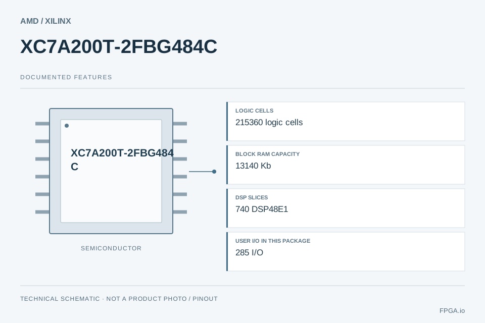
Technical schematicFPGA.io technical schematic for XC7A200T-2FBG484C. Values summarize the documented fields below; consult their source conditions. This is an abstract diagram, not a product photograph, package drawing or pinout. Parameter sources below ↓
XC7A200T-2FBG484C is an FPGA in the AMD / Xilinx Artix-7 family, supplied in the FBG484 package. Its reviewed resources include 215,360 logic cells, 13,140 Kb of block RAM, 285 I/O for this device/package combination. This ordering code specifies speed grade -2 and Commercial (C) temperature grade. The selected device/package has 4 GTP channels; check this package-level limit before planning serial interfaces. Use the linked manufacturer data sheets for electrical limits, pin assignments and timing. FPGA.io can review the complete part number for chip sourcing or a combined sourcing and PCBA project.
Compare FBG484 and SBG484 board requirements deliberately
Use these checks to prepare a design review or a sourcing request for XC7A200T-2FBG484C. The evidence rows describe the device; the actions are engineering guidance, not completed validation.
Compare FBG484 with SBG484 as different footprints
Package code
FBG484
Package body
23 x 23 mm
Ball pitch
1 mm
Check: For an FBG484-to-SBG484 change, compare official body-size, pitch and land-pattern drawings alongside your routing rules. Both labels ending in 484 does not make their pad coordinates or escape strategy interchangeable.
Prepare: A package drawing, land-pattern reference and fan-out feasibility review for the chosen option.
Check: Allocate parallel buses and serial channels separately. If the design exceeds either package limit, reducing logic utilization does not create more physical connections.
Prepare: An interface inventory with separate ordinary-I/O, dedicated-channel and reference-clock checks.
Evidence and conditions
7 Series FPGAs Data Sheet: Overview · revision 2.6.1 · p. 3, Table 5, XC7A200T row, FBG484 columns · scope: device-package. Package-specific user I/O. HR I/O; excludes serial transceiver channels.
7 Series FPGAs Data Sheet: Overview · revision 2.6.1 · p. 3, Table 5, XC7A200T row, FBG484 columns; GTP column · scope: device-package. Number of channels exposed in this selected device/package; not device-family maximum.
Use -2C as a condition, not a frequency promise
Speed grade
-2
Junction temperature (Tj)
0 to +85 °C
Temperature reference
Tj
Check: Check the Artix-7 electrical data sheet for the selected speed and operating conditions, then run timing for the actual routed design. Review cooling against the documented temperature basis.
Prepare: Timing constraints, implementation report and the operating-condition assumptions used for sign-off.
Evidence and conditions
7 Series FPGAs Data Sheet: Overview · revision 2.6.1 · p. 16, Figure 2; Speed Grade legend · scope: MPN. Retain original ordering code -2 in the literal MPN. Datasheet grade is -2. This is not a single application clock limit.
Artix 7 FPGAs Data Sheet: DC and AC Switching Characteristics · revision 1.27.1 · p. 3, Table 2 Recommended Operating Conditions (continued); Tj Commercial (C) row · scope: grade. Junction temperature Tj, not ambient temperature. Apply only to a literal MPN with the corresponding grade; not a claim all grades are available.
Artix 7 FPGAs Data Sheet: DC and AC Switching Characteristics · revision 1.27.1 · p. 3, Table 2 Recommended Operating Conditions (continued); Tj Commercial (C) row · scope: grade. Junction temperature Tj, not ambient temperature. Apply only to a literal MPN with the corresponding grade; not a claim all grades are available. Expressed from the same reviewed junction-temperature range; not an additional measurement.
Before accepting a quotation
Specify -2FBG484C on the quotation, not only XC7A200T or BGA484.
Treat SBG484, industrial grade and other speed bins as separate engineering options with their own line items.
Request an offer validity period, lot/traceability terms and an explicit shipping commitment; this page supplies no live stock or fixed price.
Availability, price, shipment date and evidence deliverables require confirmation for the actual offer. No supplier stock or replacement qualification is established by this page.
Choose the sourcing or redesign route
Existing FBG484 design: obtain an exact-code offer and validate the delivery and traceability terms.
Board area is the constraint: compare SBG484 geometry, escape routing and assembly capability before changing footprint.
Connections are the constraint: evaluate a package with sufficient exposed I/O and channels, then revise the pin and board plan.
Core device, package and grade fields are linked to official documents. The full MPN is evidenced by a historical manufacturer listing; current lifecycle and availability require confirmation. Voltage, application timing and power are not fully characterized here.
Junction temperature Tj, not ambient temperature. Apply only to a literal MPN with the corresponding grade; not a claim all grades are available. Expressed from the same reviewed junction-temperature range; not an additional measurement.
Junction temperature Tj, not ambient temperature. Apply only to a literal MPN with the corresponding grade; not a claim all grades are available. Expressed from the same reviewed junction-temperature range; not an additional measurement.
Junction temperature Tj, not ambient temperature. Apply only to a literal MPN with the corresponding grade; not a claim all grades are available. Expressed from the same reviewed junction-temperature range; not an additional measurement.
Conditional temperature operation
Not confirmed
unconfirmed
Minimum core voltage
Not confirmed
unconfirmed
Nominal core voltage
Not confirmed
unconfirmed
Maximum core voltage
Not confirmed
unconfirmed
Supply & status
Parameter
Value
Scope / evidence
Current lifecycle
Not confirmed
unconfirmedConditions
Not verified in this review.
Available stock
Not confirmed
unconfirmedConditions
Not verified in this review.
MANUFACTURER REFERENCES
Official documents & PDF datasheets
Use the electrical data sheet together with the device overview and package/pinout information.
Full ordering-number evidence: XCN20011 v1.0, p. 2, Table 4, single table block, data row 3, Replacement Part column.
Manufacturer documents may be revised. Verify the current revision and applicable device/package/grade before releasing a design.
DEVICE & PACKAGE DECISION
Compare the FBG484 footprint with compact SBG and larger FBV choices
This commercial FBG484 choice keeps the XC7A200T core resources while making the package connection budget the main board constraint. SBG484 offers a different documented body and pitch; the larger FBV676 row exposes different I/O and channel totals but also carries historical lifecycle conditions. Evaluate those differences before treating the shared device name as a migration path.
Engineering screening guidance using reviewed catalogue evidence. Examples are hypothetical and advisory; validate your actual design and the exact ordering code.
Result: 61 I/O remain in the count-only budget (78.6% allocated).
Planning diagram: assumed I/O allocation 224 I/O assumed allocation / 285 documented package I/O; 61 I/O unallocated. Count-only planning diagram, not a pinout or bank assignment.
78.6% of the sourced package count allocated; 61 I/O unallocated.
Each signal consumes one single-ended user I/O in this example. Dedicated serial lanes are separate. Bank voltage, differential pairing, clocks, configuration use and actual pin allocation can reduce usable capacity. Reserved signals here are an assumed design allowance, not manufacturer-reserved pins.
Result: Allocate at least 262,144 payload bits before adding memory overhead. The current reviewed embedded-memory reference is 13,140 Kb.
Payload arithmetic only. The source Kb/kb unit is retained; this example does not choose a decimal/binary conversion or claim a percentage fit. Round each buffer to the native memory-block geometry and check port width, depth, ECC/parity, dual-port use and implementation reports.
Public device and ordering comparisons
Compare exact package and grade conditions below. These are screening references; matching names, dimensions or resource counts do not establish pin compatibility or replacement approval.
XC7A200T-2FBG484C and already-public screening candidates
Native LUT4, LE and logic-cell metrics remain separate. Temperature is not converted to ambient; source notes define the operating basis. A family maximum is never substituted for package I/O or channels. No clock, power or stock figure is inferred.
Sources and conditions: XC7A200T-2FBG484C
Lifecycle / ordering: Not verified in this review.
Speed grade: -2.7 Series FPGAs Data Sheet: Overview · revision 2.6.1 · p. 16, Figure 2; Speed Grade legend · scope: MPN. Retain original ordering code -2 in the literal MPN. Datasheet grade is -2. This is not a single application clock limit.
Operating temperature (see basis/conditions): 0 to +85 °C.Artix 7 FPGAs Data Sheet: DC and AC Switching Characteristics · revision 1.27.1 · p. 3, Table 2 Recommended Operating Conditions (continued); Tj Commercial (C) row · scope: grade. Junction temperature Tj, not ambient temperature. Apply only to a literal MPN with the corresponding grade; not a claim all grades are available.
Temperature basis: Tj.Artix 7 FPGAs Data Sheet: DC and AC Switching Characteristics · revision 1.27.1 · p. 3, Table 2 Recommended Operating Conditions (continued); Tj Commercial (C) row · scope: grade. Junction temperature Tj, not ambient temperature. Apply only to a literal MPN with the corresponding grade; not a claim all grades are available. Expressed from the same reviewed junction-temperature range; not an additional measurement.
Body dimensions: 23 x 23 mm.7 Series FPGAs Packaging and Pinout Product Specification · revision 1.20 · p. 11, Table 1-1; p. 266, Figure 4-12, D/E dimensions · scope: package. Package body width x length; excludes PCB keep-out and component height.
Package user I/O: 285 I/O.7 Series FPGAs Data Sheet: Overview · revision 2.6.1 · p. 3, Table 5, XC7A200T row, FBG484 columns · scope: device-package. Package-specific user I/O. HR I/O; excludes serial transceiver channels.
Package dedicated channels: 4 GTP.7 Series FPGAs Data Sheet: Overview · revision 2.6.1 · p. 3, Table 5, XC7A200T row, FBG484 columns; GTP column · scope: device-package. Number of channels exposed in this selected device/package; not device-family maximum.
Logic cells (AMD): 215,360 logic cells.7 Series FPGAs Data Sheet: Overview · revision 2.6.1 · p. 3, Table 4, XC7A200T row; Logic Cells column · scope: device. Vendor metric; not comparable to another architecture's ALMs.
Embedded block memory: 13,140 Kb.7 Series FPGAs Data Sheet: Overview · revision 2.6.1 · p. 3, Table 4, XC7A200T row; Block RAM Max (Kb) column · scope: device. Source unit retained: Kb means kilobits, not kilobytes.
Sources and conditions: XC7A200T-L1SBG484I
Package: FBG484 → SBG484. Verify the applicable limits and design impact.
Temperature grade: Commercial (C) → Industrial (I). Verify the applicable limits and design impact.
Speed grade: -2 → -1L. Verify the applicable limits and design impact.
Lifecycle / ordering: Not verified in this review.
Speed grade: -1L.7 Series FPGAs Data Sheet: Overview · revision 2.6.1 · p. 16, Figure 2; note 1 · scope: MPN. Retain original ordering code -L1 in the literal MPN. Datasheet grade is -1L. This is not a single application clock limit.
Operating temperature (see basis/conditions): -40 to +100 °C.Artix 7 FPGAs Data Sheet: DC and AC Switching Characteristics · revision 1.27.1 · p. 3, Table 2 Recommended Operating Conditions (continued); Tj Industrial (I) row · scope: grade. Junction temperature Tj, not ambient temperature. Apply only to a literal MPN with the corresponding grade; not a claim all grades are available.
Temperature basis: Tj.Artix 7 FPGAs Data Sheet: DC and AC Switching Characteristics · revision 1.27.1 · p. 3, Table 2 Recommended Operating Conditions (continued); Tj Industrial (I) row · scope: grade. Junction temperature Tj, not ambient temperature. Apply only to a literal MPN with the corresponding grade; not a claim all grades are available. Expressed from the same reviewed junction-temperature range; not an additional measurement.
Body dimensions: 19 x 19 mm.7 Series FPGAs Packaging and Pinout Product Specification · revision 1.20 · p. 11, Table 1-1; p. 265, Figure 4-11, D/E dimensions · scope: package. Package body width x length; excludes PCB keep-out and component height.
Package user I/O: 285 I/O.7 Series FPGAs Data Sheet: Overview · revision 2.6.1 · p. 3, Table 5, XC7A200T row, SBG484 columns · scope: device-package. Package-specific user I/O. HR I/O; excludes serial transceiver channels.
Package dedicated channels: 4 GTP.7 Series FPGAs Data Sheet: Overview · revision 2.6.1 · p. 3, Table 5, XC7A200T row, SBG484 columns; GTP column · scope: device-package. Number of channels exposed in this selected device/package; not device-family maximum.
Logic cells (AMD): 215,360 logic cells.7 Series FPGAs Data Sheet: Overview · revision 2.6.1 · p. 3, Table 4, XC7A200T row; Logic Cells column · scope: device. Vendor metric; not comparable to another architecture's ALMs.
Embedded block memory: 13,140 Kb.7 Series FPGAs Data Sheet: Overview · revision 2.6.1 · p. 3, Table 4, XC7A200T row; Block RAM Max (Kb) column · scope: device. Source unit retained: Kb means kilobits, not kilobytes.
Sources and conditions: XC7A200T-2FBV676C
Package: FBG484 → FBV676. Verify the applicable limits and design impact.
Lifecycle / ordering: This exact V-package MPN is listed in XCN20011 as an affected discontinued product. The current lifecycle field is not refreshed from a current source.
Package: FBV676.7 Series FPGAs Packaging and Pinout Product Specification · revision 1.20 · p. 268, Figure 4-14, shared FBG676/FBV676 drawing, title · scope: package. Exact V-package token printed in the shared drawing and historical MPN; not renamed to its replacement package.
Speed grade: -2.7 Series FPGAs Data Sheet: Overview · revision 2.6.1 · p. 16, Figure 2; Speed Grade legend · scope: MPN. Retain original ordering code -2 in the literal MPN. Datasheet grade is -2. This is not a single application clock limit.
Operating temperature (see basis/conditions): 0 to +85 °C.Artix 7 FPGAs Data Sheet: DC and AC Switching Characteristics · revision 1.27.1 · p. 3, Table 2 Recommended Operating Conditions (continued); Tj Commercial (C) row · scope: grade. Junction temperature Tj, not ambient temperature. Apply only to a literal MPN with the corresponding grade; not a claim all grades are available.
Temperature basis: Tj.Artix 7 FPGAs Data Sheet: DC and AC Switching Characteristics · revision 1.27.1 · p. 3, Table 2 Recommended Operating Conditions (continued); Tj Commercial (C) row · scope: grade. Junction temperature Tj, not ambient temperature. Apply only to a literal MPN with the corresponding grade; not a claim all grades are available.
Body dimensions: 27 x 27 mm.7 Series FPGAs Packaging and Pinout Product Specification · revision 1.20 · p. 268, Figure 4-14, shared FBG676/FBV676 drawing, D/E dimensions · scope: package. Package body width x length, not die dimensions, height or PCB keep-out.
Package user I/O: 400 I/O.7 Series FPGAs Packaging and Pinout Product Specification · revision 1.20 · p. 16, Table 1-8, XC7A200T row, FBG676/FBV676 shared column · scope: device-package. HR user I/O only; excludes serial transceiver channels.
Package dedicated channels: 8 GTP channels.7 Series FPGAs Packaging and Pinout Product Specification · revision 1.20 · p. 12, Table 1-3, XC7A200T row, FBG676/FBV676 shared column · scope: device-package. Channels bonded out in this exact device/package; a blank or dash is never read as zero.
Logic cells (AMD): 215,360 logic cells.7 Series FPGAs Data Sheet: Overview · revision 2.6.1 · p. 3, Table 4, XC7A200T row; Logic Cells column · scope: device. Vendor metric; not comparable to another architecture's ALMs.
Embedded block memory: 13,140 Kb.7 Series FPGAs Data Sheet: Overview · revision 2.6.1 · p. 3, Table 4, XC7A200T row; Block RAM Max (Kb) column · scope: device. Source unit retained: Kb means kilobits, not kilobytes.
Does speed grade -2 guarantee my processing clock?
No single application clock follows from the grade. Constrain and implement the design with the applicable Artix-7 electrical data sheet and validate the selected package, operating conditions and routed paths.
What does the numerical example establish for XC7A200T-2FBG484C?
It establishes arithmetic under the explicitly hypothetical inputs shown here. It is not a tool result, synthesis report, timing closure, pin-assignment validation or application qualification. Replace the assumptions with your signal list and memory geometry, then validate in the vendor tools.
For software-heavy control with limited parallel I/O, assess an MCU or processor against the same latency, interface and power requirements. For wide parallel datapaths or custom timing, compare FPGA architectures using a mapped design. For early prototyping, an evaluation board may reduce initial hardware work; verify its exact device, accessible interfaces and production suitability.
Start with this package’s I/O, block RAM and serial channel counts, or enter your actual requirements. Native resource requirements apply only to the selected architecture.
86 full MPNs meet the entered numeric constraints. Showing 2 device representatives, at most two per manufacturer, ordered by smallest excess resources. Temperature and package variants still need selection.
Different family or manufacturer: review native logic/DSP architecture, HDL/IP portability and toolchain.
Package: FBG484 → FBG676. Verify the applicable limits and design impact.
Speed grade: -2 → -1. Verify the applicable limits and design impact.
Numeric matches do not establish pin compatibility, protocol support, lifecycle or supply availability.
Numeric screening is not replacement approval.
Logic and DSP mapping, pinout, bank voltages, temperature, timing, protocol support and toolchain remain engineering checks. Serial channel quantity does not verify data rate or protocol support. Cross-brand candidates generally require board and HDL review.