Logic implementation
39,600 LE
Use this native resource count for an initial budget. LUT, logic-cell and logic-element definitions differ; synthesize your HDL in the target toolchain to establish fit and timing.
Manufacturer evidence ↗ Conditions ↓Altera / Cyclone IV E
F23 · I · Speed grade -7
FPGA.io Part Number FIO-900D532765BF036BInternal catalogue reference · manufacturer MPN remains unchanged
Lifecycle & ordering review: Exact-MPN ordering-table presence does not establish lifecycle status. Evidence and conditions ↓
Core fields reviewed 2026-09-27
Source links and conditions accompany each parameter.
SOURCING REFERENCES
No verified supplier stock or price is currently displayed here. Request a quotation for your quantity and required delivery date.
| Platform / market | Available quantity | Unit price / quantity | Lead time | Source & checked time |
|---|---|---|---|---|
| DigiKey | View supplier source ↗ | |||
| Mouser | View supplier source ↗ | |||
| Farnell / element14 | View supplier source ↗ | |||
| Arrow | View supplier source ↗ |
Supplier references are independent of FPGA.io inventory. Confirm currency, region, quantity tier, packing, taxes, freight and final terms at source.
Search links do not establish stock, price or an authorized distribution relationship. Check the full code, package and grade at the source.
Already have a target price or delivery date? Request a Better Quote ↗
PRODUCT OVERVIEW
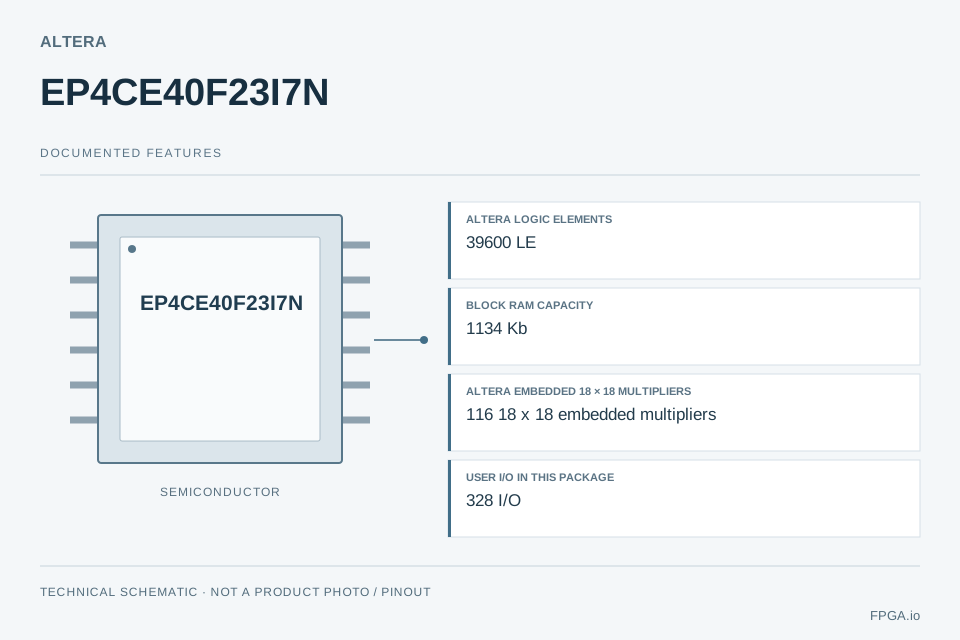
EP4CE40F23I7N is an FPGA in the Altera Cyclone IV E family, supplied in the F23 package. Its reviewed resources include 39,600 LE, 1,134 Kb of block RAM, 328 I/O for this device/package combination. This ordering code specifies speed grade -7 and I temperature grade. The selected device/package has 0 serial transceiver channels; check this package-level limit before planning serial interfaces. Use the linked manufacturer data sheets for electrical limits, pin assignments and timing. FPGA.io can review the complete part number for chip sourcing or a combined sourcing and PCBA project.
Core device/package/grade facts checked against official sources. Native resources are not cross-vendor equivalents. Detailed timing, design power and current supply status require project review.
| Parameter | Value | Scope / evidence |
|---|---|---|
| Logic cells | Not confirmed | unverifiedConditionsAltera LE count is logic_elements; no conversion to AMD logic cells. |
| 6-input LUTs | Not confirmed | unverifiedConditionsCyclone IV uses four-input LUT LEs; no LUT6 equivalence. |
| Block RAM capacity | 1134 Kb | deviceCYIV-OVERVIEW-2-0 ↗PDF p. 17 / Volume 1 printed p. 1-3, Table 1-1, EP4CE40 column; Embedded memory (Kbits) rowConditionsOfficial embedded memory Kbits including parity capacity. 1 Kb=1024 bits; not bytes. |
| 36 Kb block RAM blocks | Not confirmed | unverifiedConditionsExisting field means 36 Kb blocks; M9K count is separate in |
| DSP slices | Not confirmed | unverifiedConditionsExisting field means DSP slices. Native 18 x 18 embedded multipliers are separate. |
| Parameter | Value | Scope / evidence |
|---|---|---|
| Altera logic elements | 39600 LE | deviceCYIV-OVERVIEW-2-0 ↗PDF p. 17 / Volume 1 printed p. 1-3, Table 1-1, EP4CE40 column; Logic elements (LEs) row; PDF p. 22 FPGA Core FabricConditionsNative Altera LE count, each with a four-input LUT and programmable register. Not AMD logic cells. |
| Altera embedded 18 × 18 multipliers | 116 18 x 18 embedded multipliers | deviceCYIV-OVERVIEW-2-0 ↗PDF p. 17 / Volume 1 printed p. 1-3, Table 1-1, EP4CE40 column; Embedded 18 x 18 multipliers row; PDF p. 22 FPGA Core FabricConditionsOne 18 x 18 or two 9 x 9 multipliers per embedded multiplier block; not AMD DSP48 slices. |
| Altera M9K blocks | 126 M9K blocks | derivedCYIV-OVERVIEW-2-0 ↗PDF p. 17 / Volume 1 printed p. 1-3, Table 1-1, EP4CE40 column; PDF p. 22 FPGA Core FabricConditionsOfficial embedded-memory Kbits / 9 Kbits per M9K; includes parity capacity. |
| Parameter | Value | Scope / evidence |
|---|---|---|
| User I/O in this package | 328 I/O | device-packageCYIV-OVERVIEW-2-0 ↗PDF p. 19 / Volume 1 printed p. 1-5, Table 1-3, EP4CE40 row, F484 columns; User I/O columnConditionsUser I/O includes general-purpose I/O, dedicated clock and dual-purpose configuration pins; excludes dedicated configuration pins. See Table 1-1 note 1. |
| Serial transceivers in this package | 0 serial transceiver channels | device-packageCYIV-OVERVIEW-2-0 ↗PDF p. 22 / Volume 1 p. 1-8, High-Speed Transceivers (Cyclone IV GX Devices Only); E package matrix Table 1-3ConditionsHigh-speed serial transceivers are GX-only. E-family GPIO LVDS/SERDES pairs do not become hard serial channels. |
| Package code | F23 | device-packageCYIV-ORDERING-STANDALONE-2-0 ↗Standalone overview PDF p. 12 / printed p. 1-12, Figure 1-3; mapped only after exact MPN existence in ordering tableConditionsFineLine BGA (FBGA); package-matrix code F484. |
| Package ball count | 484 balls | packageCYIV-ORDERING-STANDALONE-2-0 ↗Standalone overview PDF p. 12 / printed p. 1-12, Figure 1-3; mapped only after exact MPN existence in ordering tableConditionsActual BGA terminal count. |
| Package body | 23 x 23 mm | packageCYIV-OVERVIEW-2-0 ↗PDF p. 19 / Volume 1 printed p. 1-5, Table 1-3, EP4CE40 row, F484 columns; Size (mm) rowConditionsBGA package size from manufacturer matrix. |
| Ball pitch | 1 mm | packageCYIV-OVERVIEW-2-0 ↗PDF p. 19 / Volume 1 printed p. 1-5, Table 1-3, EP4CE40 row, F484 columns; Pitch (mm) rowConditionsBall pitch; source package-matrix pitch. |
| Package terminals / leads (vendor count) | 484 pins | packageCYIV-ORDERING-STANDALONE-2-0 ↗Standalone overview PDF p. 12 / printed p. 1-12, Figure 1-3; mapped only after exact MPN existence in ordering tableConditionsManufacturer package pin count. BGA package: pin positions are physical balls. |
| Parameter | Value | Scope / evidence |
|---|---|---|
| Speed grade | -7 | partCYIV-ORDERING-STANDALONE-2-0 ↗Standalone overview PDF p. 12 / printed p. 1-12, Figure 1-3; mapped only after exact MPN existence in ordering tableConditionsSource speed grade; retain L because it distinguishes low-voltage grades. Not a universal Fmax. |
| Junction temperature (Tj) | -40 to +100 °C | partCYIV-DATASHEET-2-1 ↗Combined handbook PDF p. 450 / Volume 3 printed p. 1-4, Table 1-3, TJ, For industrial use; grade mapping: standalone overview p. 12, Figure 1-3ConditionsIndustrial recommended operating junction-temperature range (TJ), not ambient temperature. This normalized range is ordinary industrial operation, not the maximum temperature under every conditional operating regime. See Conditional temperature operation below when present; the baseline limits apply to ordinary rated operation. |
| Temperature grade | I | partCYIV-ORDERING-STANDALONE-2-0 ↗Standalone overview PDF p. 12 / printed p. 1-12, Figure 1-3; mapped only after exact MPN existence in ordering tableConditionsIndustrial; temperature grade does not independently establish certification. I7 conditional extended operation is recorded separately. |
| Core voltage conditions | 1.15-1.25 V | partCYIV-DATASHEET-2-1 ↗Combined handbook PDF pp. 450-451 / Volume 3 printed pp. 1-4 to 1-5, Table 1-3 VCCINT 1.2-V operation row and note 1 (I7)ConditionsNominal 1.20 V internal-logic supply for grade I7. Standard-voltage C6/C7/C8/I7/A7 grades supported at 1.2 V. |
| Maximum application clock | Not confirmed | unverifiedConditionsApplication-specific timing not reviewed. Use implementation constraints and timing analysis. |
| Application power | Not confirmed | unverifiedConditionsDesign activity, voltage and temperature dependent; no single device power asserted. |
| Minimum junction temperature | -40 °C | partCYIV-DATASHEET-2-1 ↗Combined handbook PDF p. 450 / Volume 3 printed p. 1-4, Table 1-3, TJ, For industrial use; grade mapping: standalone overview p. 12, Figure 1-3ConditionsIndustrial recommended operating junction-temperature range (TJ), not ambient temperature. This normalized range is ordinary industrial operation, not the maximum temperature under every conditional operating regime. See Conditional temperature operation below when present; the baseline limits apply to ordinary rated operation. |
| Maximum junction temperature | 100 °C | partCYIV-DATASHEET-2-1 ↗Combined handbook PDF p. 450 / Volume 3 printed p. 1-4, Table 1-3, TJ, For industrial use; grade mapping: standalone overview p. 12, Figure 1-3ConditionsIndustrial recommended operating junction-temperature range (TJ), not ambient temperature. This normalized range is ordinary industrial operation, not the maximum temperature under every conditional operating regime. See Conditional temperature operation below when present; the baseline limits apply to ordinary rated operation. |
| Temperature reference | Tj | partCYIV-DATASHEET-2-1 ↗Combined handbook PDF p. 450 / Volume 3 printed p. 1-4, Table 1-3, TJ, For industrial use; grade mapping: standalone overview p. 12, Figure 1-3ConditionsTJ, not TA. |
| Conditional temperature operation | Historical conditional extended range | part-conditionalALTERA-EXTENDED-TEMPERATURE-SUPPORT ↗Cyclone IV FPGA Extended Industrial Temperature Offerings, EP4CE40 row, base ordering code EP4CE40F23I7; N suffix applicability note above table; timing-analysis and temperature-profile conditions preceding tableConditionsTj -40 to 125 °C, operating speed -8. Historical manufacturer support table requires extended-range timing analysis with an I7 target and -40/125 C temperature settings; operating speed grade is -8 and nominal supply is 1.2 V. Manufacturer confirmation of acceptable temperature profiles is required. Do not treat -7 at 125 C as unconditional. |
| Minimum core voltage | 1.15 V | partCYIV-DATASHEET-2-1 ↗Combined handbook PDF pp. 450-451 / Volume 3 printed pp. 1-4 to 1-5, Table 1-3 VCCINT 1.2-V operation row and note 1 (I7)ConditionsGrade I7, 1.2-V operation. |
| Nominal core voltage | 1.2 V | partCYIV-DATASHEET-2-1 ↗Combined handbook PDF pp. 450-451 / Volume 3 printed pp. 1-4 to 1-5, Table 1-3 VCCINT 1.2-V operation row and note 1 (I7)ConditionsGrade I7, 1.2-V operation. |
| Maximum core voltage | 1.25 V | partCYIV-DATASHEET-2-1 ↗Combined handbook PDF pp. 450-451 / Volume 3 printed pp. 1-4 to 1-5, Table 1-3 VCCINT 1.2-V operation row and note 1 (I7)ConditionsGrade I7, 1.2-V operation. |
| Parameter | Value | Scope / evidence |
|---|---|---|
| Current lifecycle | Not confirmed | unverifiedConditionsExact-MPN ordering-table presence does not establish lifecycle status. |
| Available stock | Not confirmed | unverifiedConditionsNo stock observation; manufacturer order code is not inventory availability. |
MANUFACTURER REFERENCES
Use the electrical data sheet together with the device overview and package/pinout information.
Data sheet / device referenceCyclone IV Device Handbook, Volume 3, Chapter 1: Cyclone IV Device DatasheetPDF pp. 450-451; printed pp. 1-4 through 1-5; Table 1-3 Recommended Operating Conditions for Cyclone IV E Devices, both parts and notes. · Rev CYIV-53001-2.1 · 2016-12Official manufacturer PDF ↗Data sheet / device referenceCyclone IV Device Handbook, Volume 1, Chapter 1: Cyclone IV FPGA Device Family OverviewPDF pp. 15-27; printed pp. 1-1 through 1-13. Tables 1-1, 1-3; FPGA Core Fabric; Figure 1-3. · Rev CYIV-51001-2.0 · 2016-03Official manufacturer PDF ↗Data sheet / device referenceCyclone IV FPGA Device Family Overview - standalone chapterp. 12 / printed p. 1-12, Figure 1-3, package and grade decoding. Ordinary industrial range is separate from conditional extended-temperature operation. · Rev CYIV-51001-2.0 · 2016-03Official manufacturer PDF ↗Selection & orderingExtended Temperature Device SupportExtended Industrial Temperature Range Devices; Cyclone IV FPGA Extended Industrial Temperature Offerings; preceding Quartus timing-analysis instructions and acceptable-temperature-profile condition.Official manufacturer webpage, indexed content ↗Selection & orderingCyclone IV E EP4CE40-F23 - supported Ordering Part NumbersOrdering Part Number column; entire visible table; literal ordering strings extracted from DOM link text.Official manufacturer ordering table ↗Full ordering-number evidence: Ordering Part Number column, data row 13, literal EP4CE40F23I7N.
Manufacturer documents may be revised. Verify the current revision and applicable device/package/grade before releasing a design.
ENGINEERING SELECTION
Use the documented resources of EP4CE40F23I7N to frame a design review. The guidance below interprets the source data; it does not establish achieved system performance.
39,600 LE
Use this native resource count for an initial budget. LUT, logic-cell and logic-element definitions differ; synthesize your HDL in the target toolchain to establish fit and timing.
Manufacturer evidence ↗ Conditions ↓1,134 Kb
Budget sample buffers, FIFOs and coefficient storage in bits, then check memory block geometry, port widths, clocking and reserved capacity. External memory needs a separate interface review.
Manufacturer evidence ↗ Conditions ↓116 18 x 18 embedded multipliers
Map the required multiply/accumulate operations, operand widths and pipeline stages to the documented DSP architecture. A resource count does not establish throughput.
Manufacturer evidence ↗ Conditions ↓328 I/O
This count applies to the selected device/package. Budget required signals and spare capacity, then check bank voltages, differential pairs, dedicated pins and configuration use in the pinout guide.
Manufacturer evidence ↗ Conditions ↓0 serial transceiver channels
No dedicated serial transceiver channels are documented for this device/package. Do not assume another package’s transceiver capability applies; evaluate a different documented part or a separate interface device.
Manufacturer evidence ↗ Conditions ↓F23
Check the official footprint, pin/ball map, pitch, escape routing, power/ground distribution and assembly constraints. Package name or ball count alone does not prove pin compatibility.
Manufacturer evidence ↗ Conditions ↓-40 to +100 °C
Check whether this range is specified at junction or ambient, together with the source conditions. Estimate power and cooling for your design before selecting the temperature grade.
Manufacturer evidence ↗ Conditions ↓These are engineering evaluation directions based on documented resources, not verified reference designs or application certifications.
Evaluate state machines, parallel interfaces and I/O expansion against the documented I/O budget, bank standards and timing. Select external level shifting or interface devices where required.
Build a resource budget →Evaluate filters, sample buffering and pipelined arithmetic using the documented DSP and block RAM resources. Validate precision, memory bandwidth, clock closure and application power in the actual implementation.
Build a resource budget →Achievable clock frequency, power consumption and interface performance depend on the implemented design, operating conditions and timing closure. Use the applicable electrical data sheet and vendor analysis tools.
FROM SELECTION TO A BOARD
ENGINEERING SHORTLIST
Start with this package’s I/O, block RAM and serial channel counts, or enter your actual requirements. Native resource requirements apply only to the selected architecture.
130 full MPNs meet the entered numeric constraints. Showing 5 device representatives, at most two per manufacturer, ordered by smallest excess resources. Temperature and package variants still need selection.
39600 LE · F23 · A
Numeric matches do not establish pin compatibility, protocol support, lifecycle or supply availability.
Lattice Semiconductor
84000 LUT4 (nominal) · BG756 · Commercial (C)
Numeric matches do not establish pin compatibility, protocol support, lifecycle or supply availability.
Lattice Semiconductor
84000 LUT4 (nominal) · BG756 · Commercial (C)
Numeric matches do not establish pin compatibility, protocol support, lifecycle or supply availability.
AMD / Xilinx
162240 logic cells · FBG676 · Commercial (C)
Numeric matches do not establish pin compatibility, protocol support, lifecycle or supply availability.
AMD / Xilinx
215360 logic cells · FBG676 · Commercial (C)
Numeric matches do not establish pin compatibility, protocol support, lifecycle or supply availability.
Logic and DSP mapping, pinout, bank voltages, temperature, timing, protocol support and toolchain remain engineering checks. Serial channel quantity does not verify data rate or protocol support. Cross-brand candidates generally require board and HDL review.
Request a board and sourcing review →DEVICE & PROCUREMENT QUESTIONS
EP4CE40F23I7N is an FPGA in the Altera Cyclone IV E family, supplied in the F23 package. Its reviewed resources include 39,600 LE, 1,134 Kb of block RAM, 328 I/O for this device/package combination. This ordering code specifies speed grade -7 and I temperature grade. The selected device/package has 0 serial transceiver channels; check this package-level limit before planning serial interfaces. Use the linked manufacturer data sheets for electrical limits, pin assignments and timing. FPGA.io can review the complete part number for chip sourcing or a combined sourcing and PCBA project.
The reviewed package is F23 and the temperature grade is I. The documented operating range is -40 to +100 °C. Industrial recommended operating junction-temperature range (TJ), not ambient temperature. This normalized range is ordinary industrial operation, not the maximum temperature under every conditional operating regime. See Conditional temperature operation below when present; the baseline limits apply to ordinary rated operation. Match the complete suffix when preparing a BOM.
Use the manufacturer-hosted PDF and documentation links in Official documents on this page. The electrical data sheet, resource overview and package/pinout guide serve different purposes; check the relevant revision and tables together.
FPGA.io confirms price, available quantity, lot requirements and lead time through a quotation. Supplier references are separate from FPGA.io stock. Send your required quantity and delivery date; an optional target unit price helps us assess a price-review request. A lower price is not guaranteed.
A similar resource count does not establish compatibility. Compare package pinout, I/O-bank voltages, configuration, timing, temperature grade and tool support. The candidate screen is a starting point for engineering review, not replacement approval.
Yes, you can request chip sourcing with PCBA project review. Include the board revision, quantity, BOM readiness, programming and inspection/test requirements. The manufacturing scope and delivery are confirmed for the specific project.
CONTINUE YOUR SELECTION
Review other documented choices in this family. Package, grade and pinout may differ; these are comparison candidates, not approved replacements.
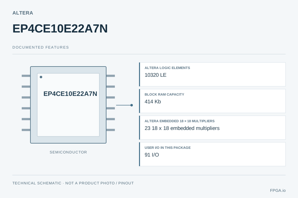
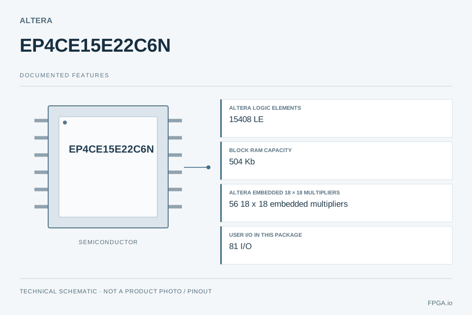
91 I/O · 414 Kb
Compare these parts →81 I/O · 504 Kb
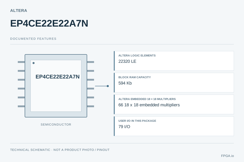
Compare these parts →79 I/O · 594 Kb
Compare these parts →ENGINEERING RESOURCES
Prepare the exact-device evidence, I/O assumptions and manufacturing scope before committing to a board.