Core fields reviewed 2026-09-27 Source links and conditions accompany each parameter.
Technical schematicFPGA.io technical schematic for EP4CE22F17I8LN. Values summarize the documented fields below; consult their source conditions. This is an abstract diagram, not a product photograph, package drawing or pinout. Parameter sources below ↓
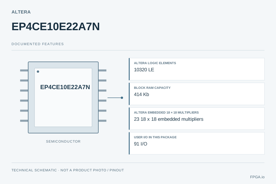
EP4CE22F17I8LN is an FPGA in the Altera Cyclone IV E family, supplied in the F17 package. Its reviewed resources include 22,320 LE, 594 Kb of block RAM, 153 I/O for this device/package combination. This ordering code specifies speed grade -8L and I temperature grade. The selected device/package has 0 serial transceiver channels; check this package-level limit before planning serial interfaces. Use the linked manufacturer data sheets for electrical limits, pin assignments and timing. FPGA.io can review the complete part number for chip sourcing or a combined sourcing and PCBA project.
Altera logic elements22,320 LE
Block RAM capacity594 Kb
Altera embedded 18 × 18 multipliers66 18 x 18 embedded multipliers
Core device/package/grade facts checked against official sources. Native resources are not cross-vendor equivalents. Detailed timing, design power and current supply status require project review.
Logic & memory
Parameter
Value
Scope / evidence
Logic cells
Not confirmed
unverifiedConditions
Altera LE count is logic_elements; no conversion to AMD logic cells.
6-input LUTs
Not confirmed
unverifiedConditions
Cyclone IV uses four-input LUT LEs; no LUT6 equivalence.
Block RAM capacity
594 Kb
deviceCYIV-OVERVIEW-2-0 ↗PDF p. 17 / Volume 1 printed p. 1-3, Table 1-1, EP4CE22 column; Embedded memory (Kbits) rowConditions
Official embedded memory Kbits including parity capacity. 1 Kb=1024 bits; not bytes.
36 Kb block RAM blocks
Not confirmed
unverifiedConditions
Existing field means 36 Kb blocks; M9K count is separate in
DSP slices
Not confirmed
unverifiedConditions
Existing field means DSP slices. Native 18 x 18 embedded multipliers are separate.
Native architecture resources
Parameter
Value
Scope / evidence
Altera logic elements
22320 LE
deviceCYIV-OVERVIEW-2-0 ↗PDF p. 17 / Volume 1 printed p. 1-3, Table 1-1, EP4CE22 column; Logic elements (LEs) row; PDF p. 22 FPGA Core FabricConditions
Native Altera LE count, each with a four-input LUT and programmable register. Not AMD logic cells.
Altera embedded 18 × 18 multipliers
66 18 x 18 embedded multipliers
deviceCYIV-OVERVIEW-2-0 ↗PDF p. 17 / Volume 1 printed p. 1-3, Table 1-1, EP4CE22 column; Embedded 18 x 18 multipliers row; PDF p. 22 FPGA Core FabricConditions
One 18 x 18 or two 9 x 9 multipliers per embedded multiplier block; not AMD DSP48 slices.
Altera M9K blocks
66 M9K blocks
derivedCYIV-OVERVIEW-2-0 ↗PDF p. 17 / Volume 1 printed p. 1-3, Table 1-1, EP4CE22 column; PDF p. 22 FPGA Core FabricConditions
Official embedded-memory Kbits / 9 Kbits per M9K; includes parity capacity.
Package & interfaces
Parameter
Value
Scope / evidence
User I/O in this package
153 I/O
device-packageCYIV-OVERVIEW-2-0 ↗PDF p. 19 / Volume 1 printed p. 1-5, Table 1-3, EP4CE22 row, F256 columns; User I/O columnConditions
User I/O includes general-purpose I/O, dedicated clock and dual-purpose configuration pins; excludes dedicated configuration pins. See Table 1-1 note 1.
Serial transceivers in this package
0 serial transceiver channels
device-packageCYIV-OVERVIEW-2-0 ↗PDF p. 22 / Volume 1 p. 1-8, High-Speed Transceivers (Cyclone IV GX Devices Only); E package matrix Table 1-3Conditions
High-speed serial transceivers are GX-only. E-family GPIO LVDS/SERDES pairs do not become hard serial channels.
Package code
F17
device-packageCYIV-ORDERING-STANDALONE-2-0 ↗Standalone overview PDF p. 12 / printed p. 1-12, Figure 1-3; mapped only after exact MPN existence in ordering tableConditions
FineLine BGA (FBGA); package-matrix code F256.
Package ball count
256 balls
packageCYIV-ORDERING-STANDALONE-2-0 ↗Standalone overview PDF p. 12 / printed p. 1-12, Figure 1-3; mapped only after exact MPN existence in ordering tableConditions
Actual BGA terminal count.
Package body
17 x 17 mm
packageCYIV-OVERVIEW-2-0 ↗PDF p. 19 / Volume 1 printed p. 1-5, Table 1-3, EP4CE22 row, F256 columns; Size (mm) rowConditions
BGA package size from manufacturer matrix.
Ball pitch
1 mm
packageCYIV-OVERVIEW-2-0 ↗PDF p. 19 / Volume 1 printed p. 1-5, Table 1-3, EP4CE22 row, F256 columns; Pitch (mm) rowConditions
Ball pitch; source package-matrix pitch.
Package terminals / leads (vendor count)
256 pins
packageCYIV-ORDERING-STANDALONE-2-0 ↗Standalone overview PDF p. 12 / printed p. 1-12, Figure 1-3; mapped only after exact MPN existence in ordering tableConditions
partCYIV-ORDERING-STANDALONE-2-0 ↗Standalone overview PDF p. 12 / printed p. 1-12, Figure 1-3; mapped only after exact MPN existence in ordering tableConditions
Source speed grade; retain L because it distinguishes low-voltage grades. Not a universal Fmax.
Junction temperature (Tj)
-40 to +100 °C
partCYIV-DATASHEET-2-1 ↗Combined handbook PDF p. 450 / Volume 3 printed p. 1-4, Table 1-3, TJ, For industrial use; grade mapping: standalone overview p. 12, Figure 1-3Conditions
Industrial recommended operating junction-temperature range (TJ), not ambient temperature. This normalized range is ordinary industrial operation, not the maximum temperature under every conditional operating regime.
Temperature grade
I
partCYIV-ORDERING-STANDALONE-2-0 ↗Standalone overview PDF p. 12 / printed p. 1-12, Figure 1-3; mapped only after exact MPN existence in ordering tableConditions
Industrial; temperature grade does not independently establish certification. I7 conditional extended operation is recorded separately.
Core voltage conditions
0.97-1.03 V
partCYIV-DATASHEET-2-1 ↗Combined handbook PDF pp. 450-451 / Volume 3 printed pp. 1-4 to 1-5, Table 1-3 VCCINT 1.0-V operation row and note 1 (I8L)Conditions
Nominal 1.00 V internal-logic supply for grade I8L. L suffix low-voltage device; C8L/C9L/I8L supported at 1.0 V.
Maximum application clock
Not confirmed
unverifiedConditions
Application-specific timing not reviewed. Use implementation constraints and timing analysis.
Application power
Not confirmed
unverifiedConditions
Design activity, voltage and temperature dependent; no single device power asserted.
Minimum junction temperature
-40 °C
partCYIV-DATASHEET-2-1 ↗Combined handbook PDF p. 450 / Volume 3 printed p. 1-4, Table 1-3, TJ, For industrial use; grade mapping: standalone overview p. 12, Figure 1-3Conditions
Industrial recommended operating junction-temperature range (TJ), not ambient temperature. This normalized range is ordinary industrial operation, not the maximum temperature under every conditional operating regime.
Maximum junction temperature
100 °C
partCYIV-DATASHEET-2-1 ↗Combined handbook PDF p. 450 / Volume 3 printed p. 1-4, Table 1-3, TJ, For industrial use; grade mapping: standalone overview p. 12, Figure 1-3Conditions
Industrial recommended operating junction-temperature range (TJ), not ambient temperature. This normalized range is ordinary industrial operation, not the maximum temperature under every conditional operating regime.
Temperature reference
Tj
partCYIV-DATASHEET-2-1 ↗Combined handbook PDF p. 450 / Volume 3 printed p. 1-4, Table 1-3, TJ, For industrial use; grade mapping: standalone overview p. 12, Figure 1-3Conditions
TJ, not TA.
Conditional temperature operation
Not confirmed
unconfirmed
Minimum core voltage
0.97 V
partCYIV-DATASHEET-2-1 ↗Combined handbook PDF pp. 450-451 / Volume 3 printed pp. 1-4 to 1-5, Table 1-3 VCCINT 1.0-V operation row and note 1 (I8L)Conditions
Grade I8L, 1.0-V operation.
Nominal core voltage
1 V
partCYIV-DATASHEET-2-1 ↗Combined handbook PDF pp. 450-451 / Volume 3 printed pp. 1-4 to 1-5, Table 1-3 VCCINT 1.0-V operation row and note 1 (I8L)Conditions
Grade I8L, 1.0-V operation.
Maximum core voltage
1.03 V
partCYIV-DATASHEET-2-1 ↗Combined handbook PDF pp. 450-451 / Volume 3 printed pp. 1-4 to 1-5, Table 1-3 VCCINT 1.0-V operation row and note 1 (I8L)Conditions
Grade I8L, 1.0-V operation.
Supply & status
Parameter
Value
Scope / evidence
Current lifecycle
Not confirmed
unverifiedConditions
Exact-MPN ordering-table presence does not establish lifecycle status.
Available stock
Not confirmed
unverifiedConditions
No stock observation; manufacturer order code is not inventory availability.
MANUFACTURER REFERENCES
Official documents & PDF datasheets
Use the electrical data sheet together with the device overview and package/pinout information.
Full ordering-number evidence: Ordering Part Number column, data row 15, literal EP4CE22F17I8LN.
Manufacturer documents may be revised. Verify the current revision and applicable device/package/grade before releasing a design.
DEVICE & PACKAGE DECISION
Check the -8L core-rail conditions before a standard-grade substitution
The F17 industrial -8L row should be considered with its sourced core-voltage range, timing designation and connection budget together. A standard -7 industrial family comparison is not a rail-equivalent substitute. Compare F23 or F29 only after checking whether their changed core, package and power conditions suit the board.
Engineering screening guidance using reviewed catalogue evidence. Examples are hypothetical and advisory; validate your actual design and the exact ordering code.
Result: 25 I/O remain in the count-only budget (83.7% allocated).
Planning diagram: assumed I/O allocation 128 I/O assumed allocation / 153 documented package I/O; 25 I/O unallocated. Count-only planning diagram, not a pinout or bank assignment.
83.7% of the sourced package count allocated; 25 I/O unallocated.
Each signal consumes one single-ended user I/O in this example. Dedicated serial lanes are separate. Bank voltage, differential pairing, clocks, configuration use and actual pin allocation can reduce usable capacity. Reserved signals here are an assumed design allowance, not manufacturer-reserved pins.
Result: Allocate at least 65,536 payload bits before adding memory overhead. The current reviewed embedded-memory reference is 594 Kb.
Payload arithmetic only. The source Kb/kb unit is retained; this example does not choose a decimal/binary conversion or claim a percentage fit. Round each buffer to the native memory-block geometry and check port width, depth, ECC/parity, dual-port use and implementation reports.
Public device and ordering comparisons
Compare exact package and grade conditions below. These are screening references; matching names, dimensions or resource counts do not establish pin compatibility or replacement approval.
EP4CE22F17I8LN and already-public screening candidates
Native LUT4, LE and logic-cell metrics remain separate. Temperature is not converted to ambient; source notes define the operating basis. A family maximum is never substituted for package I/O or channels. No clock, power or stock figure is inferred.
Sources and conditions: EP4CE22F17I8LN
Lifecycle / ordering: Exact-MPN ordering-table presence does not establish lifecycle status.
Package: F17.Cyclone IV FPGA Device Family Overview - standalone chapter · revision CYIV-51001-2.0 · Standalone overview PDF p. 12 / printed p. 1-12, Figure 1-3; mapped only after exact MPN existence in ordering table · scope: device-package. FineLine BGA (FBGA); package-matrix code F256.
Speed grade: -8L.Cyclone IV FPGA Device Family Overview - standalone chapter · revision CYIV-51001-2.0 · Standalone overview PDF p. 12 / printed p. 1-12, Figure 1-3; mapped only after exact MPN existence in ordering table · scope: part. Source speed grade; retain L because it distinguishes low-voltage grades. Not a universal Fmax.
Grade: I.Cyclone IV FPGA Device Family Overview - standalone chapter · revision CYIV-51001-2.0 · Standalone overview PDF p. 12 / printed p. 1-12, Figure 1-3; mapped only after exact MPN existence in ordering table · scope: part. Industrial; temperature grade does not independently establish certification. I7 conditional extended operation is recorded separately.
Operating temperature (see basis/conditions): -40 to +100 °C.Cyclone IV Device Handbook, Volume 3, Chapter 1: Cyclone IV Device Datasheet · revision CYIV-53001-2.1 · Combined handbook PDF p. 450 / Volume 3 printed p. 1-4, Table 1-3, TJ, For industrial use; grade mapping: standalone overview p. 12, Figure 1-3 · scope: part. Industrial recommended operating junction-temperature range (TJ), not ambient temperature. This normalized range is ordinary industrial operation, not the maximum temperature under every conditional operating regime.
Package user I/O: 153 I/O.Cyclone IV Device Handbook, Volume 1, Chapter 1: Cyclone IV FPGA Device Family Overview · revision CYIV-51001-2.0 · PDF p. 19 / Volume 1 printed p. 1-5, Table 1-3, EP4CE22 row, F256 columns; User I/O column · scope: device-package. User I/O includes general-purpose I/O, dedicated clock and dual-purpose configuration pins; excludes dedicated configuration pins. See Table 1-1 note 1.
Package dedicated channels: 0 serial transceiver channels.Cyclone IV Device Handbook, Volume 1, Chapter 1: Cyclone IV FPGA Device Family Overview · revision CYIV-51001-2.0 · PDF p. 22 / Volume 1 p. 1-8, High-Speed Transceivers (Cyclone IV GX Devices Only); E package matrix Table 1-3 · scope: device-package. High-speed serial transceivers are GX-only. E-family GPIO LVDS/SERDES pairs do not become hard serial channels.
Logic elements (Altera): 22,320 LE.Cyclone IV Device Handbook, Volume 1, Chapter 1: Cyclone IV FPGA Device Family Overview · revision CYIV-51001-2.0 · PDF p. 17 / Volume 1 printed p. 1-3, Table 1-1, EP4CE22 column; Logic elements (LEs) row; PDF p. 22 FPGA Core Fabric · scope: device. Native Altera LE count, each with a four-input LUT and programmable register. Not AMD logic cells.
Core rail reference: 0.97-1.03 V.Cyclone IV Device Handbook, Volume 3, Chapter 1: Cyclone IV Device Datasheet · revision CYIV-53001-2.1 · Combined handbook PDF pp. 450-451 / Volume 3 printed pp. 1-4 to 1-5, Table 1-3 VCCINT 1.0-V operation row and note 1 (I8L) · scope: part. Nominal 1.00 V internal-logic supply for grade I8L. L suffix low-voltage device; C8L/C9L/I8L supported at 1.0 V.
Sources and conditions: EP4CE15F23I7N
Package: F17 → F23. Verify the applicable limits and design impact.
Speed grade: -8L → -7. Verify the applicable limits and design impact.
Lifecycle / ordering: Exact-MPN ordering-table presence does not establish lifecycle status.
Package: F23.Cyclone IV FPGA Device Family Overview - standalone chapter · revision CYIV-51001-2.0 · Standalone overview PDF p. 12 / printed p. 1-12, Figure 1-3; mapped only after exact MPN existence in ordering table · scope: device-package. FineLine BGA (FBGA); package-matrix code F484.
Speed grade: -7.Cyclone IV FPGA Device Family Overview - standalone chapter · revision CYIV-51001-2.0 · Standalone overview PDF p. 12 / printed p. 1-12, Figure 1-3; mapped only after exact MPN existence in ordering table · scope: part. Source speed grade; retain L because it distinguishes low-voltage grades. Not a universal Fmax.
Grade: I.Cyclone IV FPGA Device Family Overview - standalone chapter · revision CYIV-51001-2.0 · Standalone overview PDF p. 12 / printed p. 1-12, Figure 1-3; mapped only after exact MPN existence in ordering table · scope: part. Industrial; temperature grade does not independently establish certification. I7 conditional extended operation is recorded separately.
Operating temperature (see basis/conditions): -40 to +100 °C.Cyclone IV Device Handbook, Volume 3, Chapter 1: Cyclone IV Device Datasheet · revision CYIV-53001-2.1 · Combined handbook PDF p. 450 / Volume 3 printed p. 1-4, Table 1-3, TJ, For industrial use; grade mapping: standalone overview p. 12, Figure 1-3 · scope: part. Industrial recommended operating junction-temperature range (TJ), not ambient temperature. This normalized range is ordinary industrial operation, not the maximum temperature under every conditional operating regime. See Conditional temperature operation below when present; the baseline limits apply to ordinary rated operation.
Package user I/O: 343 I/O.Cyclone IV Device Handbook, Volume 1, Chapter 1: Cyclone IV FPGA Device Family Overview · revision CYIV-51001-2.0 · PDF p. 19 / Volume 1 printed p. 1-5, Table 1-3, EP4CE15 row, F484 columns; User I/O column · scope: device-package. User I/O includes general-purpose I/O, dedicated clock and dual-purpose configuration pins; excludes dedicated configuration pins. See Table 1-1 note 1.
Package dedicated channels: 0 serial transceiver channels.Cyclone IV Device Handbook, Volume 1, Chapter 1: Cyclone IV FPGA Device Family Overview · revision CYIV-51001-2.0 · PDF p. 22 / Volume 1 p. 1-8, High-Speed Transceivers (Cyclone IV GX Devices Only); E package matrix Table 1-3 · scope: device-package. High-speed serial transceivers are GX-only. E-family GPIO LVDS/SERDES pairs do not become hard serial channels.
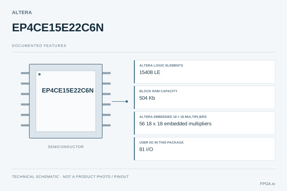
Logic elements (Altera): 15,408 LE.Cyclone IV Device Handbook, Volume 1, Chapter 1: Cyclone IV FPGA Device Family Overview · revision CYIV-51001-2.0 · PDF p. 17 / Volume 1 printed p. 1-3, Table 1-1, EP4CE15 column; Logic elements (LEs) row; PDF p. 22 FPGA Core Fabric · scope: device. Native Altera LE count, each with a four-input LUT and programmable register. Not AMD logic cells.
Core rail reference: 1.15-1.25 V.Cyclone IV Device Handbook, Volume 3, Chapter 1: Cyclone IV Device Datasheet · revision CYIV-53001-2.1 · Combined handbook PDF pp. 450-451 / Volume 3 printed pp. 1-4 to 1-5, Table 1-3 VCCINT 1.2-V operation row and note 1 (I7) · scope: part. Nominal 1.20 V internal-logic supply for grade I7. Standard-voltage C6/C7/C8/I7/A7 grades supported at 1.2 V.
Sources and conditions: EP4CE30F29I7N
Package: F17 → F29. Verify the applicable limits and design impact.
Speed grade: -8L → -7. Verify the applicable limits and design impact.
Lifecycle / ordering: Exact-MPN ordering-table presence does not establish lifecycle status.
Package: F29.Cyclone IV FPGA Device Family Overview - standalone chapter · revision CYIV-51001-2.0 · Standalone overview PDF p. 12 / printed p. 1-12, Figure 1-3; mapped only after exact MPN existence in ordering table · scope: device-package. FineLine BGA (FBGA); package-matrix code F780.
Speed grade: -7.Cyclone IV FPGA Device Family Overview - standalone chapter · revision CYIV-51001-2.0 · Standalone overview PDF p. 12 / printed p. 1-12, Figure 1-3; mapped only after exact MPN existence in ordering table · scope: part. Source speed grade; retain L because it distinguishes low-voltage grades. Not a universal Fmax.
Grade: I.Cyclone IV FPGA Device Family Overview - standalone chapter · revision CYIV-51001-2.0 · Standalone overview PDF p. 12 / printed p. 1-12, Figure 1-3; mapped only after exact MPN existence in ordering table · scope: part. Industrial; temperature grade does not independently establish certification. I7 conditional extended operation is recorded separately.
Operating temperature (see basis/conditions): -40 to +100 °C.Cyclone IV Device Handbook, Volume 3, Chapter 1: Cyclone IV Device Datasheet · revision CYIV-53001-2.1 · Combined handbook PDF p. 450 / Volume 3 printed p. 1-4, Table 1-3, TJ, For industrial use; grade mapping: standalone overview p. 12, Figure 1-3 · scope: part. Industrial recommended operating junction-temperature range (TJ), not ambient temperature. This normalized range is ordinary industrial operation, not the maximum temperature under every conditional operating regime. See Conditional temperature operation below when present; the baseline limits apply to ordinary rated operation.
Package user I/O: 532 I/O.Cyclone IV Device Handbook, Volume 1, Chapter 1: Cyclone IV FPGA Device Family Overview · revision CYIV-51001-2.0 · PDF p. 19 / Volume 1 printed p. 1-5, Table 1-3, EP4CE30 row, F780 columns; User I/O column · scope: device-package. User I/O includes general-purpose I/O, dedicated clock and dual-purpose configuration pins; excludes dedicated configuration pins. See Table 1-1 note 1.
Package dedicated channels: 0 serial transceiver channels.Cyclone IV Device Handbook, Volume 1, Chapter 1: Cyclone IV FPGA Device Family Overview · revision CYIV-51001-2.0 · PDF p. 22 / Volume 1 p. 1-8, High-Speed Transceivers (Cyclone IV GX Devices Only); E package matrix Table 1-3 · scope: device-package. High-speed serial transceivers are GX-only. E-family GPIO LVDS/SERDES pairs do not become hard serial channels.
Logic elements (Altera): 28,848 LE.Cyclone IV Device Handbook, Volume 1, Chapter 1: Cyclone IV FPGA Device Family Overview · revision CYIV-51001-2.0 · PDF p. 17 / Volume 1 printed p. 1-3, Table 1-1, EP4CE30 column; Logic elements (LEs) row; PDF p. 22 FPGA Core Fabric · scope: device. Native Altera LE count, each with a four-input LUT and programmable register. Not AMD logic cells.
Can I reuse a standard -7 core rail for this -8L code?
Compare the sourced recommended core-voltage ranges in the table and the applicable handbook conditions. A matching industrial temperature grade does not make the supply requirements equal; validate all rails and sequencing.
What does the numerical example establish for EP4CE22F17I8LN?
It establishes arithmetic under the explicitly hypothetical inputs shown here. It is not a tool result, synthesis report, timing closure, pin-assignment validation or application qualification. Replace the assumptions with your signal list and memory geometry, then validate in the vendor tools.
For software-heavy control with limited parallel I/O, assess an MCU or processor against the same latency, interface and power requirements. For wide parallel datapaths or custom timing, compare FPGA architectures using a mapped design. For early prototyping, an evaluation board may reduce initial hardware work; verify its exact device, accessible interfaces and production suitability.
Start with this package’s I/O, block RAM and serial channel counts, or enter your actual requirements. Native resource requirements apply only to the selected architecture.
292 full MPNs meet the entered numeric constraints. Showing 6 device representatives, at most two per manufacturer, ordered by smallest excess resources. Temperature and package variants still need selection.
Different family or manufacturer: review native logic/DSP architecture, HDL/IP portability and toolchain.
Package: F17 → FBG484. Verify the applicable limits and design impact.
Temperature grade: I → Commercial (C). Verify the applicable limits and design impact.
Speed grade: -8L → -1. Verify the applicable limits and design impact.
Numeric matches do not establish pin compatibility, protocol support, lifecycle or supply availability.
Numeric screening is not replacement approval.
Logic and DSP mapping, pinout, bank voltages, temperature, timing, protocol support and toolchain remain engineering checks. Serial channel quantity does not verify data rate or protocol support. Cross-brand candidates generally require board and HDL review.