
How this works
Total = single-ended signals + 2 × differential pairs + additional clock pins + reserved user I/O.
FPGA selection / T005
Add single-ended signals, differential pairs, clocks and reserved user I/O.
FBG676 · quantity not entered · service Electronic component sourcing. Return to the device evidence. This context is retained when you choose the enquiry form; it is not a completed device review.
01 / DEFINE THE REQUIREMENT
02 / REVIEW THE OUTPUT
Ready for an example run. Check the inputs, then run the tool.
Total user-I/O demand with allocation checks
The report records the tool version and calculation time. Project enquiry opens a separate form for your review; it does not submit automatically.
Silent original animation with English captions, not a recording of a hardware test or a customer session. Hypothetical LFE5U-25F-6BG256C example. No pin, timing or board qualification.
01 KEEP THE FULL MPN — LFE5U-25F-6BG256C Use the BG256 package evidence. Retain the grade and document version. Full MPN + package + source version
02 COUNT EACH SIGNAL ONCE — 32 single-ended signals 4 differential pairs use 8 pins 2 other clocks + 6 reserved user I/O 32 + (4 x 2) + 2 + 6 = 48 pins
03 CHECK PACKAGE CAPACITY — Reviewed package capacity: 197 user I/O Count margin: 197 - 48 = 149 A positive count is not bank or pin fit. Pin locations and bank voltages still need review.
04 CHANGE AN INPUT — Try a demand above package capacity. A negative margin is a count deficit. Changing inputs invalidates old results. Preserve failure results. Never silently turn unknown into zero.
05 SAVE THE ASSUMPTIONS — Save the text decision report. Keep inputs, source version and open checks. The report is not engineering approval. Your planning calculation remains local in this browser.
06 REVIEW BEFORE ENQUIRY — Choose component sourcing or PCBA. Check MPN, quantity and report in the form. Only your final submission sends the request. MPN + quantity + selected service + planning brief
03 / METHOD & VERIFICATION
Method version 1 · 2026-09-27
FPGA.io planning aid. Arithmetic and checklist output do not replace device documentation, a design tool or engineering approval.
Total = single-ended signals + 2 × differential pairs + additional clock pins + reserved user I/O.
Each count: whole number 0–1,000,000. Put each signal in only one category. Differential clocks belong in the pair count.
32 single-ended + 8 differential pairs + 2 extra clock pins + 6 reserved → 56 user I/O.
Use the example inputs to inspect how the method behaves. This is a reference calculation, not a hardware test.
Follow a worked example + editable workbook →Calculations and pasted lists stay in this browser. No account is required. An enquiry brief is stored temporarily in this tab's session only when you choose to transfer it.
Report a method or input issue →04 / CONTINUE THE TASK
Keep exact device and board revisions with the assumptions you just checked.
Continue the task with the relevant source scope. These reading paths do not establish interchangeability or current supply.
Related fpga reading and planning context; not a compatibility recommendation.
Related fpga reading and planning context; not a compatibility recommendation.
Related fpga reading and planning context; not a compatibility recommendation.
Related fpga reading and planning context; not a compatibility recommendation.
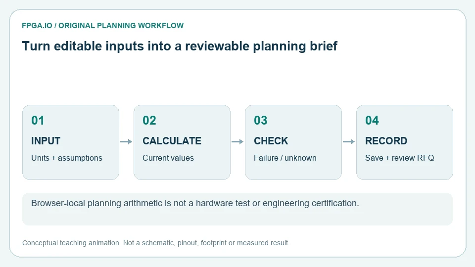
Turn editable inputs into a reviewable planning brief · Browser-local planning arithmetic is not a hardware test or engineering certification.
Original conceptual teaching visual. Not a product photograph, schematic, pinout, footprint or measured result. The static poster is used when reduced motion is requested.