
Hard-to-find
XC2VP7-6FF672C: Preserve the PowerPC, Rails and FF672 Map
Published · Updated
XC2VP7-6FF672C is a Virtex-II Pro FPGA with one embedded PowerPC processor block, eight RocketIO channels and 396 user I/Os in the FF672 package. A legacy-board purchase therefore preserves more than a logic-cell count. Processor software, configuration files, analog transceiver supplies and the actual ball map can each determine whether a recovered unit has a useful role in the released design.
This guide links the exact affected number in XCN20001 v1.1 with DS083 v5.0, 21 June 2011. It provides a resource-and-infrastructure handoff for maintaining an existing board. The examples are arithmetic and document-reading exercises. No inventory, price, delivery, authenticity, compatible substitute, hardware measurement or successful project rebuild has been established.
Request price and lead time for XC2VP7-6FF672C, 25 pieces on the homepage. Replace the example quantity with your actual requirement; it is not a minimum order, stock quantity or promised delivery.
Separate the affected code, revision and last-order deadline
The complete number appears literally in XCN20001 Table 1 on PDF page2, with “No direct replacement” in its own replacement column. The neighboring FF896 and FFG entries are different purchasing identities. Do not select a similar-looking row in the other half of the table, remove the C or insert a G to make an offered part resemble the request. The complete ordering-number tutorial explains the identity record; this page applies that discipline to a processor-bearing FPGA.
The notice was first issued on 6 January 2020. Version 1.1, dated 24 February 2020, updated some part numbers. Its revision date must remain separate from the initial issue date. Page 6 sets the last-time-buy deadline at 31 July 2020, subject to material availability, and requires final deliveries on or before 31 January 2021. These are historical manufacturer withdrawal deadlines. Neither date describes the age, availability or acceptance conditions of a present third-party offer.
The same page states that an order remaining open on or after 31 May 2020 would be non-cancellable and non-returnable. That historical manufacturer condition is not automatically a term of a new transaction. Preserve the original notice and separately record the supplier's current written terms. An old last-shipment date does not prove that every later offered lot is invalid, nor does it provide a traceable chain for any particular package. Lot evidence must answer the current purchasing question.
DS083 Module 1 Figure 1, printed page8 and combined PDF page9, explains the flip-chip ordering fields: device, speed grade, package, pin count and temperature grade. Here -6 selects the speed grade, FF672 the flip-chip fine-pitch BGA, and C the commercial junction-temperature range of 0°C to +85°C. This is Tj, not ambient temperature. A room at 85°C does not demonstrate compliance, because the powered junction can be hotter. Keep the full number in the BOM, quotation and incoming-inspection record.
The notice's no-direct-replacement entry leaves redesign open as an engineering project. It supplies no automatic cross-reference. A proposed modern FPGA may have more nominal logic and still omit the embedded processor, use different configuration storage, require different rails or demand new firmware and layout. Ask for the proposed full number and an explicit change record. An exact-part sourcing request and a redesign request can proceed as separate decisions with separate evidence and acceptance owners.
Budget the processor, fabric and rails as separate systems
Use the XC2VP7 row of DS083 Module 1 Table 1, combined PDF page2: one PowerPC block, 4,928 slices, 44 blocks of 18 Kb Block SelectRAM+, 44 dedicated 18-by-18 multipliers and four DCMs. The table also lists 11,088 logic cells and a maximum 792 Kb block-memory total. A logic-cell figure is not a directly interchangeable LUT count across FPGA generations. Preserve the resource definition when comparing a synthesis report or a proposed replacement, and keep memory-block geometry separate from an aggregate bit total.
The package-specific Table 3 on combined PDF page8 lists 396 user I/Os and eight RocketIO channels for XC2VP7 in FF672. Module 4 Table 3 independently distinguishes 396 user I/Os, 196 differential I/O pairs and 72 transceiver-related pins. The latter are nine named pins per transceiver, including supplies and analog ground; they are not 72 serial lanes. Differential-pair and user-I/O counts overlap and must not be added as separate capacities. Reserved functions can further reduce the signals available to a particular board.
Speed claims also need the correct row. Module 1 Table 4 gives a -6 flip-chip RocketIO maximum of 3.125 Gb/s and a PowerPC-block maximum of 350 MHz. These are architecture- and grade-scoped limits, not proof that a particular routed design, protocol or board meets them. The 6.25 Gb/s RocketIOX headline belongs to a different device subset. Rebuilding the design still requires its clock relationships, constraints, timing reports, transceiver configuration and interface evidence. A family headline cannot replace those inputs.
| Domain | Recommended range | Scope and unresolved work |
|---|---|---|
| VCCINT | 1.425–1.575 V | Commercial Tj 0°C to +85°C; internal core |
| VCCAUX | 2.375–2.625 V | Auxiliary circuits; retain droop and sequencing guidance |
| VCCO | 1.2–3.45 V envelope | Actual bank supply follows its I/O standard; 3.3 V requires the referenced guidance |
| AVCCAUXRX / AVCCAUXTX | 2.375–2.625 V | Virtex-II Pro column, not the adjacent Pro X receive range |
| VTRX / VTTX | 1.6–2.625 V | Termination supply entries; configuration and powering rules still apply |
DS083 Module 3 Table 2, printed page2, combined PDF page73. These are recommended operating entries, not absolute maxima or a complete power design.
The supply table uses the Virtex-II Pro column of Module 3 Table 2. The adjacent Virtex-II Pro X receive-supply entries are different; copying across the merged heading would change the requirement. VCCO's broad envelope does not permit arbitrary mixed standards within a bank. The table directs 3.3 V I/O users to XAPP659 and warns that RocketIO powering guidelines apply even when transceivers are unused. This guide has not qualified those full power guidelines, sequencing, decoupling, analog noise or board regulators.
Do not size a regulator from a typical idle-current figure. Module 3 Table 4 conditions its typical values on nominal voltage and 25°C, specifies commercial-grade scope and describes unloaded, three-state I/Os. Dynamic fabric, processor, clock, I/O and transceiver activity require separate assessment. For a maintenance purchase, retrieve the released schematic and measured operating conditions from the project owner. If those records are missing, retain a power-review gap rather than treating an apparently familiar rail label as acceptance.
Read FF672 by device column, bank and viewing direction
DS083 Module 4 Table 8 spans printed pages51–69, combined PDF pages181–199. It shares a pin-description table among XC2VP2, XC2VP4 and XC2VP7, with separate no-connect columns. A function printed in the shared description column may be unavailable on the selected device. For example, balls F25, F24, F23 and F22 are marked NC in the XC2VP7 column. Their printed I/O-like descriptions do not make them usable signals. Check the selected device column at every assigned ball.
The source reading reconciled 672 unique package positions with the selected column and the package summary. It found 396 available user-I/O positions across eight banks: banks0,1,4,5 each expose39, while banks2,3,6,7 each expose60. These are available-function counts before application reservations. They do not establish compatible I/O standards, differential pairing, reference availability or legal placement for your signals. In particular, a spare position in a distant bank cannot repair a voltage or reference conflict in the bank where an existing trace lands.
For a concrete allocation counterexample, suppose the unchanged board routes forty required single-ended user signals into bank zero. The selected-device table exposes only thirty-nine user positions there before any application reservation. That local demand already exceeds the documented count even if the whole-package worksheet reports spare positions elsewhere. A different bank assignment would be a board change, with its own voltage and routing review. This example explains why the total is an early screen rather than a pin-planning approval. It does not propose moving a particular net, assign a legal I/O standard or establish a revised layout.
Configuration can consume otherwise useful positions. Table 4 explains that SelectMAP data and control pins can become user I/Os after configuration unless the port is retained. Table 8 places shared BUSY/DOUT at AC6 and D0/DIN at AB7. Their role depends on the actual configuration mode and retention choice. Preserve the released configuration scheme, boot image and constraints alongside the board revision. Do not budget a shared function twice or erase its startup behavior from a steady-state pin spreadsheet.
Module 4 Figure 4, printed page70 and combined PDF page200, provides a dimensioned FF672 component outline. It shows a 27 mm body dimension marked basic, 1.00 mm basic ball pitch, a depopulated matrix and separate top and bottom views. The height table gives 2.45 mm nominal and 2.65 mm maximum for A. These are component-drawing dimensions, not verified PCB pad dimensions, solder-mask rules, escape routing or enclosure clearance. The simplified figure above deliberately supplies no reusable footprint.
A pin-1 marker and a bottom-view matrix cannot be overlaid casually on a top-view PCB image. Review orientation with the official drawing and the actual CAD library; then compare every used ball against the board netlist and constraints. This article's document reconciliation is not a board-level continuity check or a library approval. Assembly planning also needs finish, package condition, moisture and handling records, reflow requirements and the real stack-up. A package number alone does not approve a recovery or reballing process.
Keep resource arithmetic separate from a successful rebuild
Begin the rebuild record with the released board revision, complete BOM, FPGA constraints, source project and configuration files. Add the exact tool release, target-device files, IP revisions and licenses, processor firmware, linker settings and boot procedure that the project actually used. One embedded PowerPC block is a hardware fact; a working software image and reproducible build are separate evidence. No implementation tool, HDL simulation, synthesis, timing closure or powered board test was run for this guide.
For a processor-bearing maintenance design, ask the project owner to identify the peripheral address map, memory initialization files and software-to-hardware interface revision that belong to the released image. Record where each file came from and which board revision it serves. A source archive without its dependent files leaves a different gap from a known build that fails on a particular board. Likewise, a boot failure is an observation to investigate, not proof by itself that the offered FPGA is defective or that a substitute is compatible. Retain the programming log, observed symptom and acceptance procedure with the actual unit under review. These are proposed evidence fields; no customer project, failure diagnosis or completed test record is being reported here.
For a deliberately hypothetical slice screen, enter 4,928 available, 3,600 required and a 20% reserve in the resource-budget calculator, selecting the explicitly matching-unit category. Its floor-based target is 3,942 slices, leaving 342 between the assumed requirement and that target. This is only arithmetic in the slice unit. It neither converts logic cells into slices nor proves that the placement, memory, multipliers or timing fit. Replace the required count with an applicable implementation report before using the result for a real project.
A second hypothetical screen uses 160 single-ended signals, 64 differential pairs, 8 additional single-ended clocks and 24 reserved user-I/O positions. The I/O calculator returns 320 positions: 160 +2×64 +8 +24. That leaves 76 against the package's 396-position maximum, before bank and shared-function qualification. Count each signal once. RocketIO serial lanes use their own dedicated transceiver resources and do not belong in this SelectIO pair count. A positive total margin does not resolve the bank-by-bank allocation.
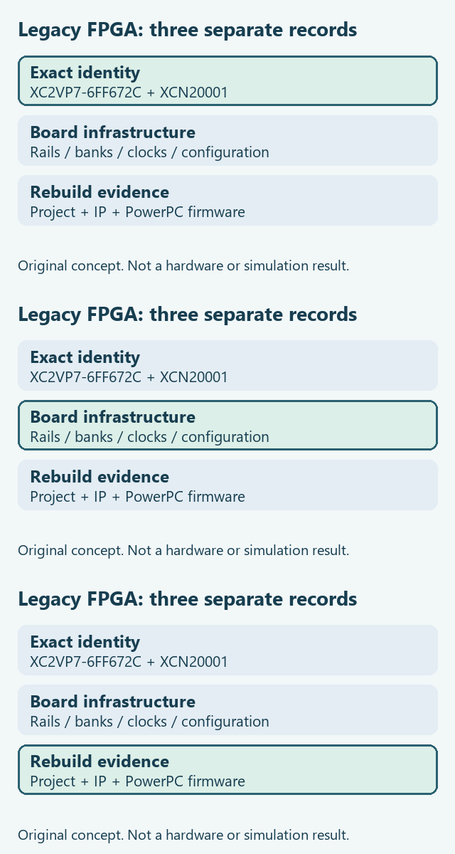
The original concept animation below separates three review records: exact identity, board infrastructure and reproducible project evidence. Its static transcript is the same sequence. None of its boxes or transitions represents a measured boot sequence, processor execution or serial waveform. Opening the animation is optional; the textual record remains the useful deliverable. Keep unresolved questions explicit rather than creating an overall compatibility score from incomplete records.
Play the original legacy-FPGA review concept
For quantity preparation, suppose one XC2VP7-6FF672C occupies U1 on each of 25 boards. The BOM checker should return 25 devices from the one-per-board line below. Correct the board quantity and reference to match the released design, and keep agreed spares separate. This tool checks the stated arithmetic and line structure; it does not establish yield, authenticity, packaging multiples, MOQ, availability or engineering suitability. A proposed alternate stays on a separate line pending its own decision.
MPN	Qty	Ref
XC2VP7-6FF672C	1	U1
Incoming evidence should identify which physical lot is being offered and tie its documents to that lot rather than to a generic catalogue description. Agree in writing which markings, packaging records, traceability documents and inspection results are required, who evaluates them and what happens when evidence is missing. This guide cannot infer provenance from a date code, photograph or seller statement alone. Preserve unanswered questions in the request instead of assigning an authenticity percentage. If an engineering substitute is proposed, keep its qualification cost and approval record separate from the exact-part quotation; a lower unit price does not settle the total maintenance decision.
The purchasing handoff should retain the exact number, actual quantity, requested delivery and destination, accepted lot documentation and owner of the substitution decision. The Hard-to-find directory provides historical notice context. The cross-reference review explains why similar pin counts cannot approve a replacement; confirm its applicable evidence before proposing a board change. For manufacturing changes, the assembly review needs actual board files and an agreed inspection and test scope, rather than this article's conceptual diagrams.
Get price and lead time for XC2VP7-6FF672C, 25 pieces. Set your actual quantity on the homepage and retain the exact requested identity. Supply evidence, a proposed redesign and board acceptance remain separate records. No present inventory, delivery commitment, direct replacement or human engineering certification is implied.
Prepared with AI-assisted manufacturer-document analysis and a separate AI review on 11 November 2026. Source revisions and historical withdrawal dates remain separately identified. No human engineering sign-off, customer project validation or hardware test is represented.