
Hard-to-find
LC4256V-10T100I: why 100 leads do not give you 100 I/Os
Published · Updated
LC4256V-10T100I contains 256 macrocells and exposes 64 general I/Os in a 100-pin TQFP package. Those are three different counts. The complete orderable number also selects the V supply family, the -10 timing grade and the industrial grade. A buyer who substitutes a nearby code can change an electrical or manufacturing condition that a short BOM description never captured.
This guide turns the original evidence into a practical handoff: an exact identity record, a package-specific signal budget and a timing example with its assumptions still attached. It uses Lattice FPGA-DS-02091 revision 23.6, January 2021, the affected-OPN workbook and the referenced package/BSDL records. It does not establish present inventory, authenticity, price, delivery, a fitted design or a ready-to-use replacement.
Request price and lead time for LC4256V-10T100I, 25 pieces on the homepage. Replace 25 with your actual requirement; this example is not a minimum order or stock claim.
What the complete label does—and does not—settle
The industrial ordering table explicitly lists LC4256V-10T100I, rather than requiring an inferred combination of suffixes. On PDF page 87, printed page 85, its row gives 256 macrocells, 3.3 V, 10 ns tPD, TQFP, 100 pins, 64 I/Os and grade I. A separate lead-free industrial table on PDF page 100 lists LC4256V-10TN100I. Keep those rows separate. LC4256V alone cannot identify the requested speed, package, grade or finish.
The exact original code also appears in AffectedOPNs_All, row 1112, column C of the manufacturer's affected-ordering-number workbook. That row identifies the SnPb line and records LC4256V-10TN100I as the historical alternative. PCN02A-15 gives an issue date of 23 June 2015, last-time-buy date of 23 December 2015 and last-shipment date of 30 December 2016. These dates describe the manufacturer's withdrawal process. They do not date a distributor's present offer or promise continuing supply.
The workbook's historical pinout, voltage and SnPb-assembly compatibility flags belong to the listed comparison at that time. They are useful evidence to preserve, not a substitution approval for a particular board or soldering process. If a supplier proposes TN100I instead, retain the requested and proposed numbers as separate fields. Review finish, assembly profile, documentation and board acceptance before changing the purchasing line. Do not silently remove or add the N to make a quote match.
A component outline is also different from a PCB land pattern. Package Diagrams FPGA-DS-02053 revision 8.8, page 68 shows the 100-pin LQFP/TQFP outline for the named families including ispMACH 4000: 14.00 mm basic body dimensions, 16.00 mm basic overall dimensions and 0.50 mm basic pitch. The tolerances, lead geometry, orientation and seating-plane notes remain part of that drawing. This article is not a fabrication footprint or permission to copy pads from another 100-pin device.
Do not infer a one-millimeter package height from a different family member. In this referenced drawing, dimension A ranges from 1.40 to 1.60 mm, with 1.50 mm nominal. Body size, overall lead span, seating-plane height and terminal pitch describe different features. Preserve the drawing datums and its notes when checking enclosure clearance or assembly access. A basic dimension is not a complete tolerance statement, and a top view is not a bottom view. A released board still needs its actual land pattern and assembly process reviewed against the applicable component drawing.
Keep the full code, notice and exact row, electrical revision, package drawing and approved board requirement in one identity record. Use the complete ordering-number tutorial when an offer or label drops a suffix. A matching base name prompts investigation; it is not acceptance evidence. Even a matching exact code does not establish what has been programmed into a delivered part, or prove the provenance and condition of its lot.
Spend 64 I/Os, not 100 package positions
The 100-pin signal tables on printed pages 50–52 have adjacent columns for 4064, 4128 and 4256 devices. Read the 4256 column throughout. This package contains 32 general I/Os in bank 0 and 32 in bank 1. Six other positions—12, 23, 27, 62, 73 and 77—carry an asterisk whose footnote says input only. Four more positions are clock/input functions: 38, 39, 88 and 89. Neither group is extra general-purpose output capacity.
The remaining terminals are four JTAG pins, four core-supply pins, six bank-supply pins and twelve grounds. Thus 64 + 6 + 4 + 4 + 4 + 6 + 12 = 100. This census was cross-checked against the original tables and the manufacturer's LC4256V 100-pin ISC BSDL model. All physical assignments agree after declared naming normalization. That source concordance is not a hardware boundary-scan test or proof that the customer's schematic has connected every terminal correctly.
Consider a deliberately simple planning example. Bank 0 needs 20 ordinary signal positions and four reserved positions; bank 1 needs the same. The general-I/O demand is 24 + 24 = 48, leaving 16 general positions unallocated before additional requirements. Two external clocks are mapped separately to documented clock/input pins. Calling this a 50-pin total is useful for a worksheet, but subtracting 50 from 64 mixes dedicated clock positions with general-I/O capacity and gives a misleading spare count.
Enter 40 single-ended signals, zero differential pairs, two other clock pins and eight spare signal pins into the I/O budget tool. The result is 50 signal pins. Zero pairs is an explicit assumption; it does not assert an FPGA-style differential interface for this CPLD. Retain the separate static record: 48 general I/Os including reserves, plus two dedicated clock/input positions. The tool counts demand; it cannot assign banks, select electrical standards or approve an interface.
Shared functions need another pass. Pin 91 includes GOE0 and pin 87 includes GOE1 in their general-I/O functions. If the design uses those enable functions, their positions are already occupied; they are not extra independent pins. Input-only positions can help genuine input requirements but cannot repair an output shortfall. The fitting report must preserve the package, banking, pin assignments and control choices. A total below 64 is an arithmetic screen for some plans, not a routing or board approval.
A -10 part has more than one timing number
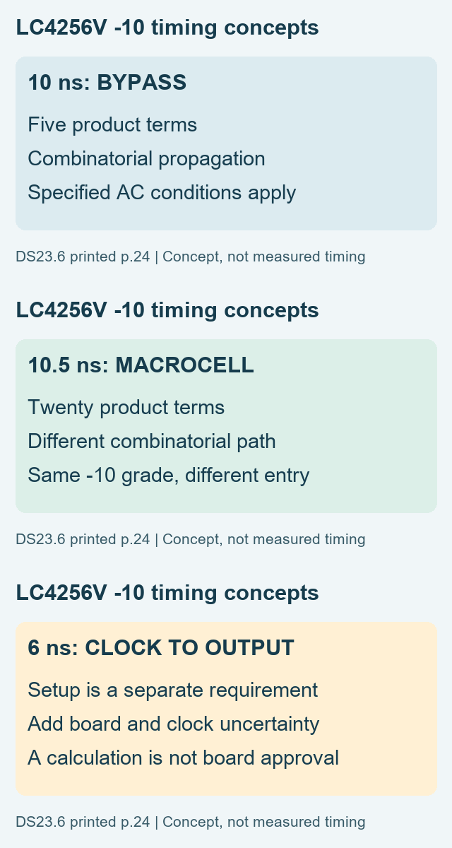
Start with the grade-specific external-switching table rather than the family's fastest headline. On printed page 24, the -10 column specifies a 10.0 ns maximum for the five-product-term bypass combinatorial path. The 20-product-term path through a macrocell has a 10.5 ns maximum. Those are different paths using different logic resources. Pasting 10 ns onto every input-to-output path loses a condition before board delay is even considered. The implemented design determines which path and loading conditions need examination.
Registered paths use other entries. The same column gives a 6.0 ns maximum GLB register clock-to-output delay and 5.5 ns minimum GLB register setup requirement. Hold requirements depend on the selected path: the input-register path does not share the same hold entry as the ordinary GLB register path. Record the actual path and its associated setup and hold parameters. Do not select a zero from one row and a setup number from another to make a spreadsheet look comfortable.
For a bounded arithmetic exercise, assume a 20 ns period, a 6 ns launching clock-to-output delay, 2 ns interconnect delay, 5.5 ns receiving setup requirement and 1 ns reserved for stated clock uncertainty. The remainder is 20 − 6 − 2 − 5.5 − 1 = 5.5 ns. Changing the assumed interconnect delay to 8 ns makes it −0.5 ns. That change demands further review. Neither result establishes hold margin, routing, clock skew, interface loading or a correct fitted implementation.
The source table's footnotes matter as much as the values. These numbers use default LVCMOS 1.8 I/O buffers and the standard switching circuit, with GRP loading of one and one output switching. Other I/O standards require the appropriate timing adjustments. Do not reuse the 5.5 ns remainder unchanged for a 3.3 V interface without reviewing those adjustments and the actual design report. Propagation delay is not the reciprocal of an application's guaranteed maximum clock frequency.
The -10 table gives 125 MHz for its specified internal-feedback counter case and 86 MHz for the external-feedback expression. These are documented test configurations, not assurances that every 256-macrocell design runs at either frequency. The family's 400 MHz headline belongs to other configurations and grades. Request the actual fitted report and constraints for LC4256V-10T100I. The cross-reference review helps prevent a similar package from being accepted without its electrical and timing work.
The original animation below compares three timing entries. It is a concept illustration, not a simulated or measured waveform. Static transcript: ten nanoseconds describes the bypass path; ten and a half describes the macrocell path; six describes clock-to-output, while setup and external assumptions remain separate. The animation does not show signal edges, reproduce a board capture or validate a clock constraint. Use the static explanation when motion is unnecessary or unavailable.
Play the original timing-entry concept animation
Close the bank, programming and purchasing records together
The V device is the 3.3 V core family; its recommended core supply is 3.0–3.6 V. The two bank-supply records are separate. For example, the I/O conditions table lists 2.3–2.7 V for LVCMOS 2.5 and 1.65–1.95 V for LVCMOS 1.8. Choosing a core voltage does not choose the correct output voltage for every receiver. Map each signal to its actual bank supply and selected standard before interpreting a family-level tolerance claim.
Five-volt input tolerance is conditional. The family documentation associates it with the applicable 3.0–3.6 V bank supply and stated interface conditions; it does not permit 5 V output logic or waive an unpowered-domain check. Industrial temperature is also specific: −40°C to 105°C is a junction-temperature range in the recommended conditions, not an ambient operating guarantee. The actual thermal path, load, clock activity and board environment must keep the junction inside its permitted range.
The JTAG electrical reference deserves its own line in the handoff. The family introduction states that the IEEE1532 interface signals are referenced to the logic-core supply, VCC. A bank configured for a lower-voltage data interface therefore does not automatically define the programming connection. Preserve the applicable cable, board-supply and programming instructions with the target selection. The published BSDL pin map is useful for checking terminal identity, but it is not the customer logic image, a speed-grade test or a measurement of the programming-voltage margin. Its file header and the product-list date also differ; retain the actual retrieved file and checksum instead of silently rewriting one date as the other. Those records make later questions answerable without pretending that a source-file comparison has tested a physical device.
A configuration file is another deliverable. Preserve the HDL or logic source, pin constraints, tool/version information, programming-file checksum and fitting/timing report targeting the complete device and package. A device identifier may distinguish a device type; it does not prove the programmed logic, speed grade, finish or provenance. Define programming and functional acceptance instead of assuming that a familiar package mark settles the design. Keep proprietary programming images and supplier records in the agreed private workflow rather than placing them in public URLs.
For a transparent quantity example, 25 boards with one CPLD per board need 25 devices before separately agreed spares or process allowances. Use the BOM checker with this exact MPN, one per board and the real reference designator. It checks supplied data and arithmetic, not schematic existence, compatibility, authenticity, yield, MOQ or packaging multiples. Keep additional quantities explicit and replace the sample reference if it does not match the released board.
For the hypothetical25-board example, paste the following three-column TSV row into the BOM checker with board count25. U3 is an example reference only; replace it with the actual released schematic reference. The expected demand is25 devices before explicit extra allowances.
MPN	Qty	Ref
LC4256V-10T100I	1	U3
If an alternative is offered, record the reason, differences, evidence needed and the owner of acceptance. Keep the historical manufacturer's suggested code beside the present offer without turning either into a direct-substitution promise. The Hard-to-find directory is a notice-led research index, not a stock feed. Use PCB fabrication or assembly review for an actual board requirement, with its applicable drawing and process documentation supplied privately.
Get price and lead time for LC4256V-10T100I, 25 pieces. The homepage keeps the full code and example quantity available for correction. For a board project, state the actual board quantity, supply responsibility and programming/test scope separately. This guide produces a documented material request and a package-specific checklist; it implies no present stock, delivery deadline, replacement qualification, hardware result or human engineering sign-off.