
Hard-to-find
LC51024MV-52F484C: Spend the Same MFB Only Once
Published · Updated
LC51024MV-52F484C is a discontinued memory-capable programmable logic device whose maximum logic and memory figures must not be added as independent resources. The original architecture spends the same multifunction blocks on different tasks. This guide helps a maintenance buyer preserve a mode-aware resource record before requesting the exact component.
It reads the ispXPLD5000MX datasheet version12.4, February2010, the PCN02A-15 notice and its affected-OPN workbook. Examples are hypothetical. No offered lot, programmed image, fitted project, board or present supply has been qualified.
Request price and lead time for LC51024MV-52F484C, 25 pieces on the homepage. Replace the quantity with your actual need. Availability, price, delivery and any alternate require confirmation.
Keep the old ordering row and the whole-family withdrawal together
LC51024MV-52F484C identifies a particular ispXPLD device, not every member of the similarly named memory-capable family. The retained February 2010 version12.4 datasheet lists this exact conventional-package code on page91: 1,024 macrocells, nominal 3.3V, a 5.2ns propagation-delay grade, 484-ball fine-pitch BGA and 317 I/O. Those are source descriptors with separate conditions. They do not establish that a new purchase contains the right configuration, that all I/O remain available, or that the maintained design meets its timing constraints.
The part-number diagram on page89 distinguishes F from FN. FN denotes the lead-free fine-pitch BGA option; removing or inserting that letter changes the requested identity. The commercial C suffix also needs its actual operating-temperature definition. Do not substitute a neighboring voltage or package code because the macrocell count looks identical. Preserve the complete requested number in the BOM, document review and quotation, and keep any proposed alternate as a separate reviewable line.
PCN02A-15 was issued on 23 June 2015. Its affected-OPN workbook, AffectedOPNs_All row1469, names LC51024MV-52F484C in Group2, the entire mature-family withdrawal group. This distinction matters: the notice also contains a different group covering selected SnPb codes in families that continued in other finishes. A purchaser cannot assume that changing this code to FN escapes the whole-family withdrawal. The retained datasheet is itself marked as discontinued; its availability as a download does not reopen factory ordering.
The notice sets last-time buy at 23 December 2015 (2015-12-23) and last shipment at 30 December 2016 (2016-12-30). These are historical manufacturer milestones, not the delivery terms of a present quotation. The worksheet points generally to MachXO2 or LatticeXP2, while recording no available specific replacement and N/A compatibility fields for this row. That is a direction for an independently scoped redesign, not an approved replacement MPN, a pin-compatible alternative, or evidence of current stock.
For maintenance work, keep three records separate: the historical withdrawal, the material actually offered, and the project that must be recovered. A correct notice can establish why the exact code is a legacy-sourcing request while leaving provenance, lot condition, programming state and delivery unresolved. The ordering-number tutorial supplies the general identity workflow. This guide adds a device-specific question: how the old project divided a finite pool of multifunction blocks between logic and memory.
| Field | Source value | Condition and locator |
|---|---|---|
| Exact OPN | LC51024MV-52F484C | PCN02A-15 workbook row1469; datasheetp91 |
| Core supply | 3.0–3.6 V | MV recommended operation; p22; not absolute maximum |
| Commercial temperature | Tj 0–90°C | Junction definition; p22, exactCgradep91 |
| Shared architecture | 32 MFB / 1024 MC maximum | Each MFB selects one mode; pp1,3 |
| True dual-port memory | 8192 bits per MFB | Legal8×1024 or16×512 examples; pp9–10 |
| Package/I/O | 484 balls / 317 I/O | ExactF484C rowp91; conditional/sharedroles |
| Propagation delay | 5.2 ns maximum | -52 five-PT bypass; defaultLVCMOS1.8 and testscopepp29–30,48 |
Allocate the 32 multifunction blocks before adding headline resources
The source selection table on page1 assigns the 51024 device 32 multifunction blocks, or MFBs, and up to 1,024 macrocells. Its maximum RAM headline is 512K bits. Reading those two maxima as independent inventories would be misleading. Page3 says that each MFB is configured in one of six modes: logic, true dual-port SRAM, pseudo dual-port SRAM, single-port SRAM, FIFO or ternary CAM. The mode selection changes what that same hardware can do.
In logic mode an MFB provides a 32-macrocell structure. In memory mode, the array and its associated paths serve the chosen memory function; page9 says unused memory-mode inputs and outputs are not accessible. A conservative planning ledger should therefore assign each block one purpose before advertising remaining logic capacity. It should not add the maximum memory capacity to the full macrocell headline. That ledger is an architecture estimate, not a reconstruction of the fitter's actual use of registers, routing or control resources.
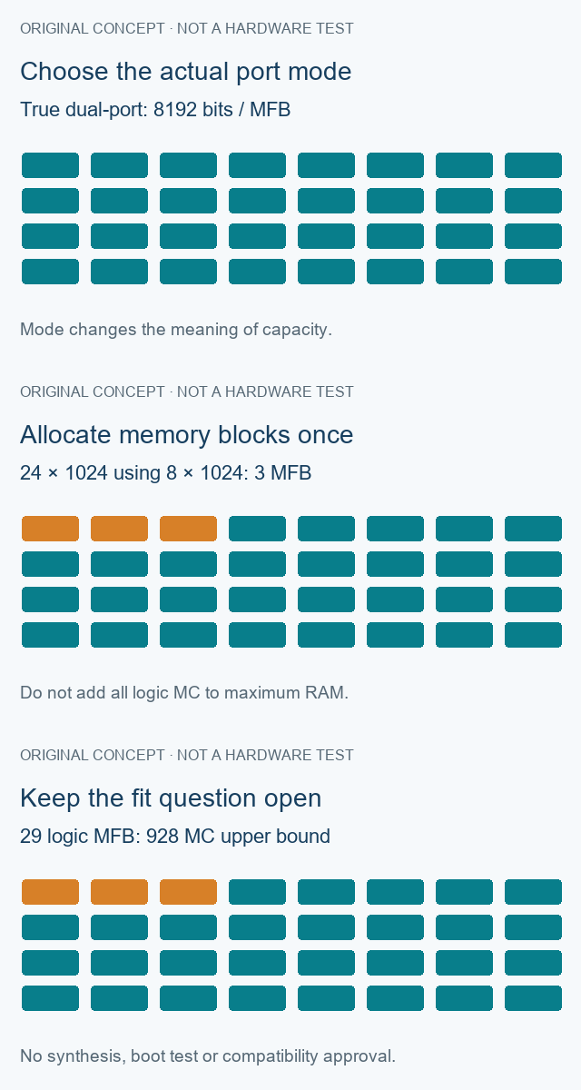
Consider a deliberately hypothetical requirement for a true dual-port buffer holding twenty-four-bit words at a depth of 1,024. Using the legal eight-by-1,024 true dual-port organization takes three width groups and one depth group, or three MFBs. Reserving those blocks for memory leaves twenty-nine blocks for logic in a simple ledger. Multiplying twenty-nine by thirty-two gives an upper-bound logic-mode count of 928 macrocells. It does not promise that 928 arbitrary equations can be implemented.
Now suppose a separate estimated logic requirement is nine hundred macrocells. Rounding nine hundred divided by thirty-two upward gives twenty-nine logic blocks. Adding three memory blocks consumes all thirty-two blocks in the arithmetic ledger, leaving no block headroom. Fragmentation, product-term structure, routing, clocks and implementation details can still make that proposal fail. The useful result is an early request for the actual implementation report and margin decision, not a green procurement approval merely because the two rounded counts add up.
Give every entry in the ledger an owner and an evidence basis. Distinguish an existing fitted report from a requirement estimate, and identify which memory instances may share resources. If port mode, depth or required clocks are unknown, leave the allocation open instead of assuming the smallest block count. A missing input is not zero. Recovering the original constraints and implementation output is more valuable than quietly changing the primitive mode until an attractive total appears.
Compare legal memory geometries within the required port mode
Table4 on page9 lists 8,192-bit true dual-port organizations, including eight bits by 1,024 words and sixteen bits by 512 words. Page10 describes two independent read/write ports accessing that same array. Its write data, address, chip select and read/write signals are registered, while outputs can be synchronous or asynchronous under the listed selections. The term dual-port therefore does not by itself mean that an arbitrary old asynchronous memory interface can be connected without changes.
For the hypothetical twenty-four-by-1,024 buffer, enter requested width 24 and depth 1024 in the BRAM organization calculator. Supply primitive width 8 and depth 1024, and select True dual-port. The geometric lower bound is three blocks, allocating 24,576 bits with no unused capacity in this arrangement. The tool accepts a vendor-supported organization supplied by the reader; it does not discover or approve the correct primitive, generate HDL, or verify collisions and clock behavior.
A second legal true dual-port organization demonstrates why the mode and shape must remain visible. Keep the same requested width and depth, but supply primitive width 16 and depth 512. Both dimensions now round up to two groups, so the lower bound is four blocks and 32,768 allocated bits, including 8,192 unused bits. Total payload size did not change. Choosing an organization can change a resource estimate even when each underlying memory block has the same bit capacity.
Single-port, pseudo dual-port and FIFO modes have a different 16,384-bit capacity per MFB. The pseudo dual-port description on page11 provides a read port and a write port, rather than two independent read/write ports. A smaller block count obtained by switching to that mode would answer a different requirement. Preserve the required operations, clocks, enables, reset behavior and initialization before comparing modes. The published Spartan-IIE memory example offers a useful contrast in primitive geometry, not a qualified substitute device.
Keep width and depth rounding separate from implementation overhead. Page9 describes wider and deeper memories, including output multiplexing for additional depth, and notes that design tools combine blocks for the specified memory size. That does not make a lower-bound calculator a fitted result. Record the selected legal mode beside each output, invalidate the result when an input is cleared, and retain a reproducible project report before relying on the remaining resources for a purchasing decision.
Read the 484-ball column without treating every position as a signal
The exact ordering row gives 484 physical balls and a 317 I/O count. These figures describe different things. The 51024 connection tables on pages76 through87 provide separate columns for 484-ball and 672-ball packages, along with primary, alternate and shared functions. The power and no-connect table on page51 must be read with them. A function present on the larger package cannot be imported into the smaller package simply because the device number matches.
The retained 484-ball document map has 332 signal-and-control positions and 152 power-and-ground positions when the tables are reconciled. The former includes fifteen dedicated control or clock positions, leaving the source's 317 I/O positions. Several I/O positions have reference-voltage, configuration or other shared duties. This count is document-reading evidence, not a free assignment list. The four dedicated global clocks, programming controls, board configuration mode and references still need their actual intended roles.
The power table distinguishes core VCC, four VCCO banks, a PLL supply, a TAP supply, PLL ground and other grounds. Its 484-ball column lists no no-connects for the 51024 density, while a smaller density in the same package has a different no-connect list. Do not copy that smaller-device list into this part's library. The source also gives a top-side orientation convention. A released component library and board-level connectivity review remain separate deliverables; no CAD library or continuity test is supplied here.
For a hypothetical user-signal budget, enter two hundred single-ended signals, forty differential pairs, zero additional user-pin clocks and sixteen reserved I/O positions in the I/O budget tool. It returns 296 user-count positions. The four dedicated clock inputs stay outside this example's user-I/O sum. Comparing 296 with the table's 317 leaves twenty-one arithmetically, but does not prove forty valid differential pairs, a legal bank allocation, or availability of reference and configuration-shared positions in a real board.
The manufacturer's archived package-diagram and BSDL links did not yield current files in this source check. No body-size tolerance, ball pitch, land pattern, stencil, reflow profile, scan-chain implementation or assembly release is inferred from the number 484. Keep those manufacturing questions open and request the released original board and package documents. If an assembly review is needed, agree its input files and acceptance scope rather than treating this article's role count as a footprint approval.
Keep commercial temperature, bank supplies and timing paths separate
The exact MV code is the nominal 3.3V version. The recommended operating table on page22 gives core VCC from 3.0V to 3.6V and the corresponding PLL-supply range for that voltage version. It defines commercial operation as junction temperature from zero to ninety degrees Celsius. This is not an ambient-temperature rating, and a different family's commercial range must not be imported. Thermal conditions and power in an actual enclosure still need a separate assessment.
Page26 sets standard-specific I/O-supply and reference conditions. LVCMOS3.3 and LVTTL use a 3.0V to 3.6V VCCO range; other supported interfaces have different requirements. The nominal core supply does not automatically specify every bank voltage. Absolute Maximum Ratings footnote5 on page22 additionally limits I/O with input voltage above 3.6V to sixty-four. This stress-table constraint is not operating permission; the applicable input standard and bank conditions, including the 3.3V-bank scope on page2, still govern use. A family headline about five-volt tolerance is therefore not permission to connect all 317 I/O to arbitrary five-volt signals.
The 5.2ns value in the exact ordering row needs its path definition. Page29 identifies it as the minus-fifty-two grade's maximum data propagation delay through the five-product-term bypass path. The PTSA path has a separate 6.5ns maximum. Page30 bases the timing table on default LVCMOS1.8 buffers, stated routing and loading, and one switching output; other standards require timing adjusters. Keep those qualifiers with a comparison instead of presenting 5.2ns as an end-to-end delay for any board connection.
The source contains separate frequency limits for internal feedback, external feedback, RAM, FIFO and CAM operations. Those are not a single project clock guarantee. A reciprocal of propagation delay also does not establish system frequency. Recover the constrained implementation and timing reports for the actual mode and paths. The power-rail workbook can organize assumed rails and loads, but its arithmetic cannot validate bank legality, hot socketing, switching noise, junction temperature or the regulator under an actual transient.
Retain the operating table, the applicable timing row and the project assumptions as different records. Absolute maximum ratings are stress limits and must not become normal rail setpoints. Typical current is not an upper-bound regulator specification. If the old design relies on an uncommon signaling mode or a special timing exception, preserve the original configuration and supporting report. No waveform, static timing run, thermal measurement or interface-compatibility test was performed for this guide.
Preserve programming evidence and quantity through the homepage inquiry
The source's nonvolatile configuration array and its reconfigurable SRAM control space answer different questions. Page20 describes the transfer of retained configuration at power-up and programming through the IEEE1532 interface; sysCONFIG provides another route for SRAM configuration. A correctly marked replacement component does not establish possession of the customer's application image. Ask which image, options, tool environment, scan chain and verification procedure belong to the maintained board before assuming a purchased part can simply be installed.
Page22 specifies a minimum of one thousand erase/reprogram cycles under the stated commercial-temperature scope. That finite nonvolatile endurance figure should not be replaced by the family's broad language about repeated SRAM reconfiguration. Page21 also describes a security setting that prevents readback and affects programming and verification until the device is erased. Do not erase a potentially valuable programmed device merely to inspect it. Identify the authorized recovery procedure and preserve the available project evidence first.
Build a handoff with four independently closeable records: exact component and lot identity; the MFB mode ledger and implementation output; the released board pin, bank and manufacturing documents; and the configuration image with its programming and test scope. Name the responsible reviewer for each. A source row can close a historical identity question while the programming file remains missing. Combining all four into one approved checkbox would hide the work still required and overstate what procurement has established.
For a deliberately hypothetical build of twenty-five boards with one LC51024MV-52F484C at U1, the BOM checker should return twenty-five components from the example row. Spares, process loss, minimum order and pack rounding remain separate requirements until explicitly entered. Preserve the exact number and actual quantity when opening the homepage inquiry. A correct multiplication confirms the example's quantity arithmetic; it says nothing about blank or programmed state, source reliability, available inventory, price or a delivery promise.
Use the Hard-to-find directory to return to the historical evidence and reviewed exact-model route. If the original part cannot meet the authorized requirement, treat a different family as a redesign proposal with its own resource mapping, board changes, tool recovery, programming and test costs. The old worksheet's general family suggestions cannot approve that proposal. The next useful purchasing action is a clearly scoped exact-part request with the missing evidence identified, while private design files remain outside public query strings.
MPN	Qty	Ref
LC51024MV-52F484C	1	U1
The original animation shows a conceptual sequence: identify the selected mode, spend each multifunction block once, and preserve the fitted-project question with the inquiry. It is not a waveform, simulation, programming log or measured resource report. The static explanation remains available when motion is hidden.
Play the original MFB allocation concept
Get price and lead time for LC51024MV-52F484C, 25 pieces. Set the actual quantity and identify the exact-part, traceability, programming and test requirements. This opens a reviewable request; no inventory or engineering approval is implied.
Prepared with AI-assisted manufacturer-document analysis. A separate AI source, full-text and visual review was completed before release. No human engineering sign-off, project build, programming verification or hardware test is represented.