
Hard-to-find
XC2S100E-6FG456C: Ask Which Power-On Branch Applies
Published · Updated
XC2S100E-6FG456C is an obsolete Spartan-IIE FPGA whose startup evidence deserves a separate check from its ordering number. The manufacturer distinguishes earlier and improved power-on behavior within the applicable device group. An exact MPN is therefore a starting identity, not proof that an offered lot can use the lower current branch or that a legacy board will start correctly.
This guide reads DS077 v3.0, 9 August 2013, the exact affected row in XCN12026 v1.0.2, and bounded mechanical and startup references. Its outputs are a lot-applicability question, an exact-package connection budget and a memory-geometry exercise. No offered material, regulator, project build, timing simulation, powered board or present supply has been tested.
Request price and lead time for XC2S100E-6FG456C, 25 pieces on the homepage. Replace the quantity with your actual need and retain exact-part requirements. The example is not an MOQ, available inventory or a delivery promise.
Preserve the full ordering number and the actual withdrawal dates
DS077 page6 distinguishes the device, speed, package and temperature fields. The requested code contains XC2S100E, the standard-performance minus-six grade, a 456-ball fine-pitch BGA and the commercial C range. The temperature definition is junction temperature, not room or ambient temperature. Keep the complete requested identity through the BOM and quotation. The ordering-number tutorial explains the general process; the startup evidence below adds a question that the ordering number alone cannot answer.
The standard FG456 package and Pb-free FGG456 option are separately identified in the ordering section. Do not insert the extra G or remove it as a spelling cleanup. A proposal with a different finish, package, speed or temperature field needs its own documented review. The marking discussion also limits dual-mark guarantees to the stated combinations; it does not make every marked part interchangeable. Photographs and traceability records should identify what is actually offered, without turning a top mark into an authenticity certificate.
XCN12026 page2 Table2 explicitly names XC2S100E-6FG456C and states that there is no direct replacement. The notice was first issued on 19 November 2012; the retained version is dated 24 April 2013, when an LTB typo was corrected. Last-time buy was 31 May 2013, with final shipment on or before 30 September 2014. Those dates describe the manufacturer withdrawal, not a current supplier delivery window. A later datasheet remaining downloadable does not reopen factory ordering.
The notice also gives historical non-cancellable, non-returnable treatment for orders placed after 31 March 2013. Preserve that historical condition separately from the terms of a new quotation. For maintenance procurement, ask for the exact full code, required quantity, agreed lot evidence and the board revision being maintained. A redesign is a different authorized task. The absence of a direct replacement in this notice must remain visible instead of being filled with a similar-looking FPGA name.
| Field | Source value | Condition and locator |
|---|---|---|
| Full code | XC2S100E-6FG456C | XCN12026 v1.0.2 p2 Table2; no direct replacement |
| Commercial temperature | Tj 0–85°C | Junction, not ambient; DS077 pp6,32 |
| Nominal core operating band | 1.71–1.89 V | 1.8 V ±5%; separate lower-voltage note not nominal timing; DS077 p32 |
| Package user-count pins | 202 | 198 ordinary I/O + four clock/user-input pins; DS077 pp5,73–89 |
| Block memory | 10 × 4096 = 40,960 bits | Legal port geometry and arrangement still apply; DS077 pp15–16 |
| Power-on current capability | 300 mA after / 500 mA before PCN | Commercial device group, minimums; lot applicability unresolved; DS077 p33 |
| Physical package | 456-ball FG456 | Standard finish; not FGG456 or footprint approval; DS077 p6, PK034 |
Ask which power-on branch applies to the offered lot
DS077 page33 is especially relevant to an old-board purchase. For commercial XC2S50E through XC2S300E devices, the listed minimum core-supply capability during power-on is three hundred milliamperes after PCN2002-05 and five hundred milliamperes before that change. The page associates the improved version with T preceding the date code and the earlier version with S. This is a source applicability distinction; it is not evidence that a particular lot has been inspected or belongs to either branch.
The same table separates ramp requirements. For the improved branch it lists a minimum of five hundred microseconds. For the earlier branch it lists two to fifty milliseconds, with the earlier measurements using core and I/O supplies powering simultaneously. The ramp is measured from ground to the nominal core voltage on a loaded board, and the source prohibits negative dips. Unknown marking or unclear lot documents should leave the branch unresolved. Selecting the smaller current merely because it is easier for the board would conceal the missing evidence.
A deliberately hypothetical supply able to provide four hundred milliamperes illustrates the question. Its stated capability is numerically above the improved branch minimum and below the earlier branch minimum. That comparison does not approve the regulator: its loaded ramp, transient behavior, protection circuit, temperature and other loads still matter. It only shows why a procurement handoff should request the applicability record. Neither table minimum is a maximum FPGA draw, and a continuous current rating is not a measured startup result.
XAPP450 v1.1 explains power-on surge and warns that overcurrent protection can interrupt startup. Its introduction says that it uses the improved specifications and sends readers to the device datasheets for specific details. Keep that limitation when reading the application note alongside DS077. Do not use an application-note example to erase the earlier-device row. The useful output is an assigned evidence request and a controlled board test plan, not a completed pass mark or a claim that a replacement purchase will cure an existing failure.
Read the separate XAPP450 v1.1 startup application note with the DS077 device-specific rows and their limitations.
A proposed startup review record can identify the actual board revision, populated loads, regulator model and protection settings, the observed device marking, and the source branch being evaluated. It should preserve the loaded core-rail waveform and the measurement setup rather than just a final voltage or an unloaded supply screenshot. Record the applicable temperature, power-up sequence, observation points and the responsible reviewer with the agreed acceptance criteria. A document reading can define that record; it cannot fill in the missing observations. A successful startup on one unit would not by itself establish the identity or behavior of every unit in a different lot. Keep the scope of any real report tied to the material and conditions it actually covers.
Count the FG456 connections from the XC2S100E column
DS077 page5 gives 202 available user-count pins for XC2S100E in FG456, including four global-clock/user-input pins. Reading the exact device column across pages73 through89 separates 198 ordinary I/O from those four input-capable clock pins. The remaining physical positions include ten dedicated control pins, twenty core-supply pins, thirty-two bank-supply pins, fifty-six grounds and 136 no-connect positions. These categories total 456; the package number is not a count of freely assignable bidirectional signals.
The device-specific column matters even when several densities share a package heading. On page89, the conditional notes make D4, D19, W4 and W19 no-connects for XC2S100E, although they are core-supply connections on the larger stated devices. A second note similarly distinguishes several ground positions. The full source map was read for this record, but the count is not a CAD library or a board continuity result. Do not wire a smaller device by copying the larger-density supply list without applying those notes.
For a hypothetical connection list, enter 170 single-ended signals, eight differential pairs, two additional single-ended clocks and eight reserved user-count positions in the I/O budget tool. It returns 196 positions. Comparing that with 202 leaves six positions arithmetically. It does not establish a legal assignment: check which signals need output capability, which need global clocks, the bank and reference-voltage constraints, and which shared configuration pins remain occupied in the real design.
PK034 v1.3 provides separate corner-gate and pin-gate mold drawings for FG456 and FGG456. The drawing uses a twenty-two by twenty-two matrix with depopulated positions, a one-millimetre basic pitch and a twenty-three-millimetre basic body dimension. A matrix dimension is not a complete occupied-ball map. The later drawing does not identify the mold option of an offered older lot. Match the released component library, orientation and actual assembly evidence; no land-pattern, stencil, reflow, clearance or manufacturing release is represented here.
PK034 v1.3 package drawing is a mechanical source, separate from the electrical pinout and the released PCB footprint.
Budget the original four-kilobit RAM geometry
DS077 page3 lists 600 configurable logic blocks and 2,700 logic cells for XC2S100E. These are different manufacturer resource units, and the typical system-gate range is another convention rather than a project utilization result. Do not compare a gate headline directly with a synthesized LUT count from a later architecture. Keep the original project target, primitive usage and implementation reports with the review. A source resource table can identify a plausible task, but cannot recreate a missing build.
Pages15 and16 give ten block memories of 4,096 bits each, totaling 40,960 bits. The listed port geometries include eight bits by 512 words and sixteen bits by 256 words. This is the original four-kilobit primitive, not an eighteen- or thirty-six-kilobit memory block borrowed from a modern FPGA. Distributed RAM is a separate resource. The actual port arrangement, clocks, collisions and initialization behavior still need to match the application and its supported primitive.
For a hypothetical twenty-four-bit-wide, 1,024-word payload, set the BRAM organization calculator to requested width 24, depth 1024 and legal primitive width 8, depth 512. Three width groups times two depth groups gives six blocks. Their allocated capacity equals 24,576 bits, leaving four of the ten source blocks arithmetically unused. This lower bound is not a mapped memory implementation, a bandwidth measurement or a timing result. Record the selected port mode and retain the implementation check.
A useful counterexample changes the payload to nine bits by 513 words while keeping the same eight-by-512 primitive mode. Width and depth each round up to two groups, so the result is four blocks, allocating 16,384 bits for a 4,617-bit payload. The unused 11,767 bits show why total bit capacity alone can mislead. This exercise describes hypothetical geometry rather than a recommended buffer architecture; blank inputs must remain unknown and must not leave a previous result looking current.
Keep voltage, temperature and -6 timing conditions together
DS077 pages6 and32 identify commercial junction temperature from zero to eighty-five degrees Celsius and nominal core voltage of 1.8V with a five-percent band, or 1.71V to 1.89V. The operating table has a separately conditioned lower-voltage functional note with a delay penalty; it is not permission to keep nominal timing at an arbitrary lower rail. Absolute maximum ratings and configuration-retention levels answer other questions. They should not become normal regulator setpoints or substitutes for operating conditions.
FG456 has eight independent I/O supply banks under the rules on pages11 and12. Each bank has four supply balls in the package listing, and all supply pins of a bank must use its required voltage. An overall I/O supply range does not make every signaling standard valid across that range. The selected output standard, input threshold supply and any reference requirement must be checked together. Use the power-rail workbook to organize the actual assumptions; its arithmetic does not verify bank legality, startup surge or a power waveform.
The minus-six field also needs its actual timing context. Page35 lists a representative global-clock-to-output maximum of 4.6ns for XC2S100E without the DLL under the stated LVTTL, drive, slew and load conditions. The source specifies a 1.4V output measurement point and a 35pF external load for the maximum. Its introductory text directs designers to the implementation static timing analyzer for precise, guaranteed project data. Taking the reciprocal of that single delay would not produce the frequency limit of an arbitrary design.
DS077 page20 describes the ISE development environment, implementation and verification flow. Preserve the actual tool release, device files, constraints, libraries, IP and generated artifacts needed by the maintained project. No particular software installation, licence, cable or old operating system was tested for this guide, and no project was rebuilt. If that environment is missing, the next task is recovery and controlled reproduction. A newer installed tool or an unchanged-looking bitstream filename does not establish the same implementation.
Turn the open questions into a purchasing handoff
Keep the FPGA configuration task separate from component identification. The source describes external configuration and multiple loading modes; an unconfigured FPGA does not contain the customer application simply because its label matches. The published XC17V04PC20C boot-memory guide illustrates the separate blank/programmed-state problem. That reading link does not qualify that PROM as a working partner for this FPGA, approve a bitstream or replace the applicable board configuration procedure.
For a deliberately hypothetical build of twenty-five boards with one XC2S100E-6FG456C at U1, the BOM checker should return twenty-five components from the row below. Keep spares, losses, minimum order and pack rounding outside that count until they are explicit requirements. The exact FPGA stays separate from its configuration memory and other board devices. A correct multiplication cannot confirm provenance, start-up suitability, package finish or available inventory.
The handoff can assign four unresolved records: lot and PCN applicability, exact board pin and bank plan, reproducible project and configuration files, and the agreed inspection or powered-test scope. Name an owner and an acceptance output for each. A seller document can close an identity question while a rail test remains open; merging those questions into one approved checkbox would hide useful information. Keep private design files and images out of shared query strings and use an agreed secure transfer route where required.
The Hard-to-find directory organizes the historical withdrawal evidence and the reviewed exact-model route. If the work expands to a board change, the assembly review needs released board files, package evidence and a defined programming and test scope. Request the exact part when the board is fixed. Treat any alternate FPGA, package or finish as a separate proposal with stated redesign and validation costs. Neither the source notice nor these calculations approve a substitute, a current supply claim or a completed engineering change.
MPN	Qty	Ref
XC2S100E-6FG456C	1	U1
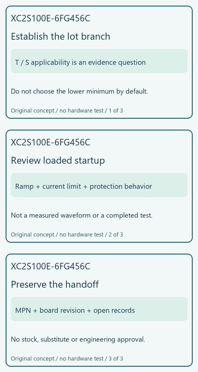
The original animation separates the lot-applicability question, the loaded startup review and the purchasing record. Its static transcript is: establish which source branch applies; review the actual board ramp and protection; preserve the evidence and unresolved items with the inquiry. It is a conceptual sequence, not a measured waveform, a completed lot inspection or a successful boot test.
Play the original Spartan-IIE startup evidence concept
Get price and lead time for XC2S100E-6FG456C, 25 pieces. Set the actual quantity on the homepage and provide the delivery, destination, lot evidence and exact-part requirement. Supply, price, delivery and any proposed alternate remain to be confirmed; the inquiry is not an engineering release.
Prepared with AI-assisted manufacturer-document analysis. A separate AI source, full-text and visual review was completed before release. No human engineering sign-off, hardware test, project build or compatibility certification is represented.