
Hard-to-find
ispPAC-POWR1014A-02T48I: Separate ADC Completion from Gate-Drive and Pin Status
Published · Updated
Customer task: recover the power-sequencing and telemetry requirements of a legacy board before buying ispPAC-POWR1014A-02T48I or accepting a substitute. The output is a review record that keeps ordering identity, ADC completion, HVOUT mode and measured board behavior separate. This is a source-based repair and sourcing guide, not a tested reference design.
1. Keep A, -02 and T48I as separate decisions
The complete code occurs in the conventional-package ordering table of Lattice FPGA-DS-02089 v2.3, October 2020, p50. The A option provides the ADC and I²C/SMBus interface. The -02 performance option includes the 12 V high-voltage FET-driver setting. T is the conventional 48-pin TQFP code; TN denotes the separate lead-free option. Do not remove these characters while searching stock or comparing a supplier offer. The documented industrial operating range is −40 to +85 °C ambient, not a junction-temperature interchangeability claim.
For lifecycle evidence, PCN02A-15 was issued on 2015-06-23. The associated workbook, sheet AffectedOPNs_All, row 2183, column C, lists this exact T48I code in 1_SnPB_Only. Column E gives ispPAC-POWR1014A-02TN48I as the historical potential alternative. The notice lists last-time buy 2015-12-23 and last shipment 2016-12-30. Those dates are historical, not a current ordering window.
The row's historical compatibility flags do not approve today's lot, process or board. The lead-free candidate's current lifecycle and availability require fresh confirmation. For the non-A, -01 variant, use the separate POWR1014-01T48I sourcing review; do not transfer its capabilities into this A/-02 requirement. The broader hard-to-find component workflow explains how to retain exact requested and offered codes.
2. Recover the ADC completion rule, not just its register addresses
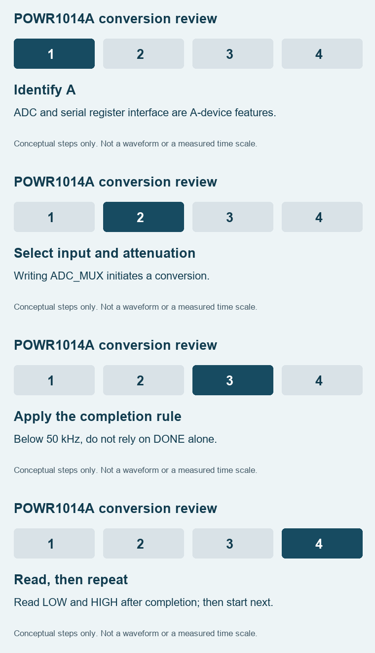
The A device has a 10-bit ADC. The interface selects a monitored input and attenuation through ADC_MUX; writing that register starts a conversion. The result is read through ADC_VALUE_LOW and ADC_VALUE_HIGH. Record the firmware sequence and the selected channel before changing hardware. A register read that succeeds on the bus is not evidence that the analog sample is ready.
DS pp11 and 28–29 recommend waiting for conversion completion before issuing a second request. Below 50 kHz I²C clock, the DONE bit is not guaranteed to indicate completion; the documented conversion-time wait must be used. Page 7 gives TCONVERT as 100 µs in the maximum column, and the operating description requires the full interval when using the timed path. Do not reinterpret this as a minimum bus frequency or claim that equality at 50 kHz is a verified firmware boundary. Confirm the applicable timing and bus conditions against the source.
Hypothetical firmware review: a board requests a new channel every 60 µs and assumes every preceding sample is valid. That schedule leaves 40 µs less than the cited 100 µs conversion interval; it cannot establish a completed conversion for every request. Fix the completion logic and capture the request/read order before concluding that an offered device is faulty. This example excludes bus-transfer overhead and is not a measured throughput figure.
The 6.144 V theoretical attenuated full scale must not be used as permission to apply that voltage to a VMON pin. Page 7 limits the high input range by the pin rating; its printed 5.9 V entry carries footnote 2. Review input limits, attenuation, error conditions and board scaling together. The worksheet should record the observed input and expected engineering units, rather than merely the raw ADC code.
Show the conversion review animation and static sequence
3. Treat the 12 V setting as one condition in the gate-drive review
HVOUT1 and HVOUT2 can operate as digital open-drain outputs or as high-voltage FET drivers. The mode is part of the programmed configuration. The -02 option does not force either pin to 12 V. In FET-driver mode the cited table provides nominal 6, 8, 10 and 12 V settings; the 12 V row gives 11.5 V minimum and 12.5 V maximum under the data-sheet conditions. Lattice FAQ 521 specifically ties the -01/-02 difference to gate-driver mode.
Gate-to-source voltage is VGS = Vgate − Vsource. In an assumed circuit with a 12 V gate and a 5 V source, VGS is 7 V. If the source rises to 10 V while that gate remains at 12 V, VGS becomes 2 V. These arithmetic examples do not establish MOSFET conduction or permissible load current. Check the actual MOSFET's gate limits and on-resistance conditions, gate charge, driver current, source trajectory and desired ramp behavior. Threshold voltage alone does not qualify a low-loss switch.
Keep FET-driver rows separate from digital-output pull-up voltage and loaded low-level limits. Obtain the programming file or a controlled reconstruction of it. A procurement line stating only “12 V driver” cannot replace a channel-by-channel mode and configuration record. Use the power-rail planning worksheet to organize supply names and sequencing assumptions; its output is a planning record, not device programming or a current estimate.
4. Observe the pin and the load, not only OUTPUT_STATUS
DS p29 explains that OUTPUT_STATUS reflects the logic signal driving an output, rather than sampling the electrical level at the pin. A high-status bit therefore cannot prove that a pull-up rail exists, a trace is connected, a FET is conducting or the load supply has reached its target. Preserve the distinction in fault reports: command state, measured output, measured rail, and board operating mode are separate observations.
For this A package, the source pin table and top view identify HVOUT1 at pin 15, HVOUT2 at pin 14, SDA at pin 38, SCL at pin 39 and RESETb at pin 40. Pin 19 is TDISEL; the revision history records an earlier diagram correction. These references help locate a source check; the teaching diagrams here are not a wiring guide or footprint. Read the complete pp3–4 pin descriptions and p51 top view against the actual board orientation.
Also separate power-on reset, blank-device, programming and normal operation. AN6075 v01.1 describes these states; a sample that has not received the required configuration cannot be evaluated as though it were the running board image. Record configuration identity, programming result and the exact state in which each observation was taken. Use a controlled startup and fault test plan, with equipment and limits appropriate to the board.
5. Decide between original-code sourcing, a candidate and a redesign
Original-code route: request ispPAC-POWR1014A-02T48I, actual quantity and delivery need. Ask for offered-code confirmation, lot traceability, storage/handling evidence and agreed inspection or test scope. Do not assume the part is programmed for your board. Stock, price, delivery and lot documentation remain subject to quotation.
Historical-candidate route: retain ispPAC-POWR1014A-02TN48I as a different ordering string. Verify lead finish and the actual assembly process, board fit, supplies, configuration support and acceptance tests. The historical row is a starting point for engineering review, not a present guarantee. The POWR1220 trim-profile review illustrates why a different power-manager architecture needs its own configuration analysis; it is not a proposed substitute for this part.
Redesign route: turn the legacy behavior into an explicit requirement: rail thresholds, ordering, timeout rules, fault actions, restart states, telemetry and external FET behavior. Replacing only the monitor count would leave essential behavior unspecified. Take the resulting board revision, programming and test requirements into a PCB assembly scope review. No path is approved solely because two packages have 48 leads.
6. Export the identity record and attach the engineering worksheet
Start with a component quantity, not a reel count. In the example, request 25 pieces of ispPAC-POWR1014A-02T48I and enter the supplier's full offered code separately. If TN48I is offered, preserve that difference. Mark source evidence checked only after reading the applicable document and entering its revision and exact locator. The tool prepares a text record and a GET inquiry link; it does not send a request or approve the candidate.
Compare requested and offered Power Manager codes
Enable JavaScript for the downloadable identity worksheet, or copy the static record below.
Static worksheet and no-script fallback
Manufacturer: Lattice
Requested MPN: ispPAC-POWR1014A-02T48I
Offered full MPN:
Component quantity:
Source / revision / page or affected row:
Board revision / configuration identifier:
HVOUT1 mode and setting / HVOUT2 mode and setting:
ADC channel / attenuation / completion method / bus clock:
Command status / measured output / measured rail / operating state:
Lead finish / assembly process / outstanding lot evidence:
Open checks / responsible reviewer / disposition:
Keep blank entries unresolved. An exact code match addresses identity only; it cannot settle condition, provenance, programming or engineering acceptance. For a scoped sourcing request, carry this record into the exact-code quotation form and replace the example quantity with your requirement before submission.
Source trail and review boundary
Official Lattice ispPAC-POWR1014/A data sheet, FPGA-DS-02089 v2.3: pp3–7, 11, 23, 27–29, 49–51 and 53. Archived October 2020 revision reviewed; verify the revision applicable to a final design. The documents and the original affected workbook support the specific historical and technical statements above; they do not document current supply.
- PCN02A-15, 2015-06-23, pp1–3; associated workbook AffectedOPNs_All row 2183, columns C and E, group 1_SnPB_Only.
- AN6075 v01.1, Power Manager II startup behavior, pp1–4.
- Lattice FAQ 521, -01 versus -02 gate-driver setting distinction.
Copy additional original source addresses
PCN: https://edge.sitecorecloud.io/latticesemi9e32-latticesemi06bb-prod9ecc-d341/media/Project/Lattice/LatticeSemi/Documents/ProductChangeNotification/PCN15/PCN02A15SnPbandSelectMatureFamilyDiscontinuance.pdf?sc_lang=en
AN6075: https://www.latticesemi.com/view_document?document_id=22087
FAQ 521: https://www.latticesemi.com/en/Support/AnswerDatabase/5/2/521
Prepared and reviewed with AI assistance on 2026-11-13; not human engineering certification. All numerical scenarios and original diagrams are educational. No board test, current inventory, delivery commitment or substitution approval is asserted.