
Hard-to-find
ispLSI 2032VE-110LT48: Screen the Actual Fitter Path Before Reusing a 48-Lead Board
Published · Updated
Use this guide with a board bill of materials, a retained fitter report, and the receiver timing requirement. It helps you decide whether a documented bypass path or an ordinary propagation path changes the timing screen for the exact ispLSI 2032VE-110LT48. The examples use assumed board delay and reserve, and the result remains a screening decision until the actual path and conditions are verified.
Resolve the historical ordering record
Start with the complete code in the original ordering table. PDF page 15 of the Lattice 2032VE data sheet lists ispLSI 2032VE-110LT48 under commercial conventional packaging, with the 48-pin TQFP package. The designation key describes L as low power, T48 as the conventional 48-pin package and a blank final temperature suffix as commercial. Treat those meanings as specific to this source. Do not replace a missing final suffix with the letter I, and do not turn T48 into TN48 in an inquiry.
The cover sheet is dated June 2010 and concerns a different earlier notice for selected devices. It calls this exact conventional orderable at that time. The later PCN 02A-15, dated 2015-06-23, and its affected workbook give the subsequent event. AffectedOPNs_All row 318 column C spells the exact order and groups it under the full-family exit. The notice records 2015-12-23 for last-time-buy orders and 2016-12-30 for last shipment under its historical terms. Neither date supplies a present lead time.
The workbook records conventional SnPb TQFP with 48 leads. The line says no compatible alternative was available there, and its pinout, voltage and assembly compatibility fields are not applicable. The words ispMach 4000V or MachXO are a family-level direction on that row. They do not specify an orderable board substitute. A later design proposal needs a complete alternative code, a documented footprint and voltage plan, a fresh fit, and board verification.
Keep a copy of the original order and the notice locator together in the repair ticket. If a distributor omits LT48 or offers a physically similar model, first establish whether it is an exact repair or a separate engineering proposal. A stock photograph, lot claim or title shared by several family members cannot close the identity question. The exact part identification guide offers a way to preserve the ordering string while the offer and traceability evidence are still being checked.
Identify the resources that the fitted board actually uses
The data sheet describes a device with thirty-two general-purpose I/O positions, two dedicated input functions and three dedicated clock positions. Some of those special functions share physical leads with programming or reset functions. Read the pin map before translating a feature count into board pins. Do not add every function count to the general-purpose I/O total. An inherited design can depend on the use of a particular dedicated pin even when plenty of programmable I/O remain.
The functional description divides the logic into Generic Logic Blocks, with signals distributed through a Global Routing Pool and outputs routed through an Output Routing Pool. The detailed blocks matter because using a bypass or a registered route can change what the timing table covers. A legacy design name is useful for finding the original project. It tells you little about the placed path without the fitter and timing reports from that project.
Draw a small inventory of inputs, registered outputs, global output enables and clocks. Keep the actual logical name and physical pin number beside each entry. A net that changes behavior between normal operation and in-system programming needs two mode labels on the same row. Write separate columns for required normal behavior and permitted programming behavior. The register, enable and reset expectations should remain visible throughout the review.
As a preliminary use of the I/O budget tool, suppose twenty single-ended data signals, four unrelated control signals and four reserved positions share the programmable I/O pool. Enter twenty-four under single-ended signals, zero differential pairs, zero additional clock pins in that pool and four reserved. The result is twenty-eight out of thirty-two, with four general-purpose positions unassigned in the example. Actual dedicated clock choices and the mode-dependent pin map still need their own check.
Separate the two propagation rows
In PDF page 7, printed page 6, table 2-0030B lists the minus-110 column. The maximum data propagation delay for the stated four-product-term and output-routing bypass case is 10.0 ns. The other data propagation row gives 13.0 ns maximum. These rows are separate source conditions. To select the bypass row, verify that the retained report establishes both bypass conditions. Keep the ordinary row or a marked unresolved estimate if you cannot trace the route.
The table applies over the recommended operating conditions and refers to switching test condition A for these delays. PDF page 5, printed page 4, shows condition A with a 316-ohm and 348-ohm test network and a 35 pF capacitance. Treat the test circuit as part of the source for the result. The data sheet's timing footnote provides the default routing, loading and clock assumptions unless a row overrides them. A board receiver, fixture or trace may differ.
Use the trace delay worksheet to estimate the board travel contribution separately. For a hypothetical 30 mm trace and assumed propagation of 150 mm/ns, one-way travel is 0.2 ns. Suppose the available launch-to-receiver screening window is 12 ns and reserve 1 ns for uncertainty. Adding the stated example terms gives 11.2 ns with the bypass path and 14.2 ns with the ordinary row. Against that chosen window, the first leaves 0.8 ns and the other exceeds it by 2.2 ns.
This arithmetic shows why selecting the wrong row could reverse an early decision. It leaves the source switching conditions, actual signal integrity, receiver threshold, clock phase, measurement error and path implementation for further review. If the board reserve already includes the trace contribution, avoid charging it twice. Keep the reason for the selected reserve and the exact reference points in the worksheet so someone else can repeat the calculation.
A registered path needs a different worksheet. On the same source page the minus-110 setup rows give a minimum of 5.5 ns for the stated four-product-term bypass case and 7.5 ns for the ordinary case. The clock-to-output maximum is 5.0 ns with the stated output-routing bypass and 6.5 ns in the other row. Begin with the actual launch register and capture boundary. Applying the combinational number to that whole route would skip the setup condition and can double count a path that the fitted report already covers.
The same table lists internal feedback, external feedback and maximum toggle frequency under different definitions. The minus-110 column shows 111 MHz in the internal feedback row and 77 MHz in the external feedback row. The internal test uses a standard sixteen-bit counter with Global Routing Pool feedback. A measured or guaranteed application frequency requires the path, test conditions and architecture that apply to your design. Keep those frequency rows separate from the path delay example.
| Fitter path | Source delay | With trace and reserve | Screen |
|---|---|---|---|
| Both bypasses | 10.0 ns max | 11.2 ns | 0.8 ns left |
| Ordinary data path | 13.0 ns max | 14.2 ns | 2.2 ns over |
Play the timing-path concept animation
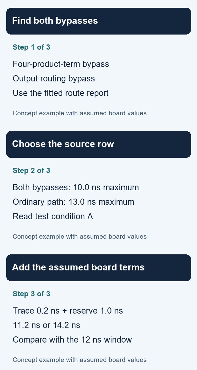
Static explanation. Confirm both bypasses in the fitter report. Use the applicable 10.0 ns or 13.0 ns source maximum, add trace and reserve once, then compare with the example 12 ns window. The animation depicts arithmetic and route selection.
Check physical leads and programming mode
PDF page 14, printed page 13, gives a top-view drawing for the exact 48-lead package style. It labels the body as 7.0 by 7.0 mm and the lead pitch as 0.5 mm. PDF page 12, printed page 11, lists signal locations for several package options in neighboring columns. The 44-pin TQFP and 44-pin PLCC columns can help identify differences, but their positions do not transfer to the 48-pin footprint. Make the 48-pin column the reference for the worksheet.
The 48-pin column lists VCC at 6 and 30 and ground at 18 and 42. Four positions, 12, 24, 36 and 48, carry the no-connect restriction. The remaining leads consist of thirty-two general-purpose I/O and eight special-function positions. The table names those special roles as GOE0, Y0, RESET/Y1, BSCAN, TDI/IN0, TMS/NC, TDO/IN1 and TCK/Y2. Count the physical positions once even when the functional name changes with mode.
BSCAN at 7 selects the programming behavior when driven low. The 48-pin column places TDI/IN0 at 8, TMS/NC at 32, TDO/IN1 at 19 and TCK/Y2 at 29. In normal mode the alternate functions apply where the signal table states them. Keep the no-connect rule for TMS in normal mode. Before changing a programming fixture or reusing a board pull network, determine whether each signal is driven during startup, programming or normal service and review the original tool instructions.
Build the pin worksheet in two passes. First record the package function and physical lead from the source with no board mapping. Then add the board net and observed connection from the actual design. If lead 32 has a board trace, establish whether it is a programming connection with the required mode behavior before placing it on the normal signal list. Treat an open question differently from the permanent no-connect positions. A continuity result alone does not identify which mode controls a pin.
Record the actual board orientation, reference designator and mapped signals alongside the source drawing. The drawing gives the source dimensions and numbering for a review. A production pad layout still needs the exact package drawing, assembly rules, courtyard, solder process and board clearance. Record which artifact actually controlled the original design. The PCB bring-up checklist helps stage power and programmed function checks after the board assumptions are settled.
Keep normal operation and production checks separate
The recommended operating table on PDF page 4, printed page 3, gives a commercial ambient temperature range from 0 to 70 °C and a 3.0 to 3.6 V supply. Read the commercial row for this exact suffix. Absolute maximum storage, case and junction stress values belong to a different table and serve a different purpose. A board environmental target needs measurements or justified estimates at the appropriate locations for the actual load and enclosure.
The input-high range and the output electrical conditions describe different directions of a signal path. The recommended table lists 2.0 V as its minimum input-high voltage and extends that input range to 5.25 V. That row does not guarantee a matching output swing into another device. Evaluate the receiving threshold, source output under load, power sequencing and any injected current in the actual circuit. A supply label on a component does not resolve all logic-level comparisons.
A receiving device may also have a different power-up timeline. Record which rail is established when the source can drive its outputs and which signal controls release. Check the source and receiving documentation together for their behavior in that interval. The design decision should identify a safe observation point and expected behavior. Leave any unverified power-off behavior open. A timing comparison made with both devices fully powered does not answer what happens during reset, programming or rail transition.
Carry the rail assumptions into the power rails worksheet. Record the intended device supply and the minimum and maximum voltage at its pins over the operating load. Allow for drops and tolerances in the board path. The condition to verify is the voltage at the part while the circuit operates. Check the actual programming power requirements separately if the board uses a different supply arrangement during that step.
If the earlier reports are unavailable, gather the project source, exact tool version, equations, selected pin constraints and programming artifact from the released assembly record. Confirm that the fit and its timing report belong to the same revision. An archived device data sheet gives input to the review. A frozen toolchain, missing image, unverified programming state or undocumented board rework can still prevent a repair decision. Record these blockers before treating an offer as usable.
Prepare a repair quantity with a clear acceptance record
For a repair that keeps the original footprint and fitted design, record ispLSI 2032VE-110LT48 exactly on the inquiry. Include the required number of boards, devices per board and any separately chosen repair spares. In the BOM checker, a deliberately simple example of twenty-five boards with one device per board yields twenty-five units. Keep inspection samples or rejected material as separate assumptions rather than allowing a hypothetical worksheet to set the real order quantity.
When preparing the quantity, record whether failed assemblies are already counted in the repair batch and whether inspection consumes separate pieces. Keep the service team and buyer working from the same arithmetic. For example, a count of boards in a repair queue is useful only when each board revision calls for the same exact position and package. Splitting orders by board revision can expose a substitution mistake before it is copied into receiving instructions.
Ask the supplier to identify the offered full code, marking and lot traceability with evidence appropriate to your repair. The current offer, storage history, lead finish and device programming condition remain to be established for the delivered lot. The manufacturer workbook helps explain the old conventional finish and discontinuation. Its row does not authenticate a seller label, determine solderability or establish that material is available now.
If a family migration is being considered, use the family names in the notice to begin a separate design inquiry. Build an explicit comparison of the original fit and proposed implementation with a complete code, logic allocation, programmer requirements, supply and pin constraints. Start a separate test record for any change in the schematic, footprint, programmable logic or manufacturing process. Keep that investigation out of the exact-part request until engineering decides what the revised design needs.
The deliverable from this review is a repair ticket with the exact order, one justified timing assumption, the package and programming checks still needed and the chosen quantity. Use the Hard-to-find directory to locate the historical notice again, or take your full order and quantity to the homepage inquiry when ready. Update the document locator when a verified revision changes the engineering conclusion.
Prepare an exact-part inquiry for ispLSI 2032VE-110LT48 with an editable example quantity
Prepared with AI assistance. The source evidence and manuscript received independent AI review. The examples describe planning arithmetic and archive evidence, not human engineering certification or measured board performance.