
Hard-to-find
74FCT162244ATPVG: Audit Four Enables Before a 5 V Bus Handoff
Published · Updated
74FCT162244ATPVG is a 5 V, 16-bit unidirectional buffer with four independent active-low output enables. It is not a bidirectional transceiver, and a TTL-compatible input does not make its outputs safe for every FPGA bank. For an obsolete-board purchase, the useful question is which signal group owns the bus, at what voltage and after which enable transition.
This guide combines the exact affected ordering number with a group-ownership worksheet and a bounded handoff calculation. The manufacturer links the exact 74FCT162244ATPVG product page to the 74FCT162244T datasheet, DSC-5461/9, September 2009. Its military and industrial columns must remain separate. Nothing here establishes current inventory, provenance, price, delivery or a qualified replacement.
Request price and lead time for 74FCT162244ATPVG, 25 pieces on the homepage. Replace the example quantity with your actual requirement; it is not a stock claim or minimum order.
Keep the complete code with the affected row
The exact product page identifies the A speed grade, a 48-lead PVG48 SSOP package, a 5 V core supply and tube carrier. Preserve the complete number as supplied. A short line such as “162244 buffer” leaves the speed and package unresolved. Do not silently add a trailing carrier code, swap PVG for PAG or accept a different timing grade because the base function sounds familiar. The complete ordering-number tutorial explains why a purchasing identity needs more than a family name.
The original PLC230018 notice lists this exact number on PDF page 32. The cached A2 addendum retains the same affected row: notice issue 3 January 2024, last-time-buy 3 July 2024 and last shipment 3 January 2025. The row's replacement, similar or redesign field says “None.” See the original manufacturer notice. The A2 revision date is a different record from the original issue date assigned to this row; it does not move either withdrawal deadline.
“None” means this notice supplies no alternative for this particular affected line. It does not prove that an engineering redesign is impossible, nor does a different document's historical recommendation establish a suitable replacement today. A proposal still needs its own complete code, electrical limits, package evidence and acceptance owner. The cross-reference review worksheet helps retain those unresolved dimensions instead of approving a device on pin count alone.
These dates describe the manufacturer's historical withdrawal process. They do not establish when a distributor acquired a lot, whether a quoted lot is authentic, or whether the offered quantity is available for delivery. Keep present sourcing questions separate from the notice record: required quantity, delivery date, destination and agreed lot evidence. Preserve the requested and offered numbers side by side if they differ. A seller's shortened description is a question to resolve, not a reason to rewrite the original requirement.
The package description has a narrower use here. The exact product page establishes SSOP and PVG48, but this guide does not supply a verified dimensioned package outline, a tolerance stack or a PCB land pattern. Do not fabricate pads or approve assembly clearance from the functional diagram below. Obtain the applicable mechanical and manufacturing records for the actual board before approving a package change. This article deliberately leaves that manufacturing decision open rather than treating a package label or catalog dimensions as a drawing.
Write down four owners before wiring sixteen bits
Datasheet page 2 shows four non-inverting, four-bit groups. Each group has one active-low output-enable input, four A data inputs and four Y three-state outputs. When that group's enable is low, its outputs follow its inputs. When the enable is high, that group's outputs enter the high-impedance state. This is a direction-specific buffer function. There is no direction-select pin that turns a Y terminal into the reverse data input of a transceiver.
The complete terminal partition is 16 A inputs, 16 Y outputs, four enable inputs, four VCC terminals and eight grounds: 48 physical positions. That count prevents two mistakes. Sixteen bits do not mean sixteen total signal connections, and four independent enable inputs are not extra data channels. The source drawing is a top view. Any board-level check must retain orientation and the correct physical terminal mapping; the conceptual drawing here is neither a pinout nor a footprint.
Create one ownership record per group. For group 1, record the source driving 1A1 through 1A4, the receivers connected to 1Y1 through 1Y4, and the controller driving 1OE. Repeat for groups 2, 3 and 4. Record whether an output is dedicated to its receiver or shares a net with another driver. If two sources can reach a common net, their permission to drive must be mutually consistent. High impedance is a state of an output; it does not erase another driver's connection or prove the shared net has a valid logic level.
As a concrete planning example, suppose twelve data bits are used and the fourth group is unused. The first three groups still need explicit enable ownership. The unused group's enable and A inputs also need a deliberate board-level disposition according to applicable design guidance. Do not infer a defined startup state or internal pull-up from the absence of a drawn external resistor. This source review has not established powered-off protection, a default enable level or a board's reset behavior. Mark those questions unresolved until the actual circuit and appropriate documentation answer them.
The same record should identify the two devices' power states during reset, programming and shutdown. A logically disabled group can still have electrical constraints at its terminals. A functional truth table is not permission to apply arbitrary voltages when a supply is absent. Ask who drives each enable during those intervals and how that level is established. A clean ownership record makes the subsequent timing review possible; a blank entry is an unknown, not a guarantee that no other source will drive.
A two-volt input threshold does not clamp a five-volt output
| Parameter | Value and category | Applicable condition | Datasheet page |
|---|---|---|---|
| VCC | 4.5–5.5 V operating range | Industrial, 5.0 V ±10% | 3 |
| Temperature | TA −40°C to +85°C | Industrial ambient, not junction or military | 3 |
| Input levels | VIH ≥2.0 V; VIL ≤0.8 V | Specified operating range | 3 |
| Output levels | VOH ≥2.4 V; VOL ≤0.55 V | Industrial IOH −24 mA / IOL +24 mA, VCC minimum, inputs VIH or VIL | 3 |
For the industrial operating range, datasheet page 3 states ambient temperature TA from −40°C to +85°C and VCC of 5.0 V ±10%, equivalent to 4.5–5.5 V. Do not inherit the adjacent military temperature range. These are operating conditions, distinct from the absolute maximum ratings on page 2. The latter describe stress limits and do not provide a functional operating recommendation or an interface acceptance rule.
The specified input-high threshold is 2.0 V minimum and the input-low threshold is 0.8 V maximum under the applicable operating range. A controller's guaranteed output levels can therefore be compared with the buffer's input requirements. That comparison needs actual guarantees at the selected load, supply and temperature. Merely calling the controller “3.3 V” does not supply its minimum output-high level, maximum output-low level, startup behavior or permitted injection current.
The Y output needs a different comparison. The industrial output-drive rows specify VOH of at least 2.4 V at −24 mA and VOL no more than 0.55 V at +24 mA, at the stated minimum supply and input conditions. A typical VOH figure of 3.3 V is not an output-voltage maximum or a protective clamp. It cannot justify connecting Y directly to an FPGA input whose permitted voltage has not been checked. Input recognition by this 5 V buffer and voltage tolerance of its receiving device are separate questions.
Work each direction explicitly. In a hypothetical controller-to-buffer connection, compare the controller's guaranteed output-high and output-low values with this device's input thresholds. Then, on the buffer-to-receiver connection, compare the buffer's full applicable output behavior with the receiver's operating and absolute limits, including power states. If the receiver's limits are missing, the result is unresolved. No subtraction of nominal rail labels can turn the missing receiver evidence into a safe margin.
Output current numbers also retain their test scope. Do not add sixteen nominal drive currents and advertise that sum as a board-level continuous-current allowance. Package power, simultaneous switching, supply integrity, external load and actual device limits still matter. The source describes balanced drivers and current-limiting resistors, but this does not automatically remove external signal-integrity work. Evaluate trace geometry, loading and required edge behavior for the actual bus. The correct deliverable is a documented interface review, not a universal claim that a series resistor is unnecessary.
Budget enable transitions separately from data propagation
| A-grade entry | Minimum / maximum | Scope | Datasheet page |
|---|---|---|---|
| Data propagation tPLH / tPHL | 1.5 / 4.8 ns | A to Y, 74FCT162244AT | 5 |
| Output enable tPZH / tPZL | 1.5 / 6.2 ns | Active-low enable to output, AT column | 5 |
| Output disable tPHZ / tPLZ | 1.5 / 5.6 ns | Active-low control returning high, AT column | 5 |
Source test scope for this table: CL 50 pF, RL 500 ohm, stated operating range and page 6 test circuit/waveforms. Page 5 notes distinguish guarantees and testing; do not infer an application frequency.
The A-grade switching table on page 5 specifies 1.5–4.8 ns for data propagation from A to Y. It separately lists 1.5–6.2 ns output enable and 1.5–5.6 ns output disable. Keep the AT column; the CT and ET columns have different maxima. These figures use the stated 50 pF load and 500 ohm resistance with the source test circuit and waveforms on page 6. They are not interchangeable descriptions of a single universal delay.
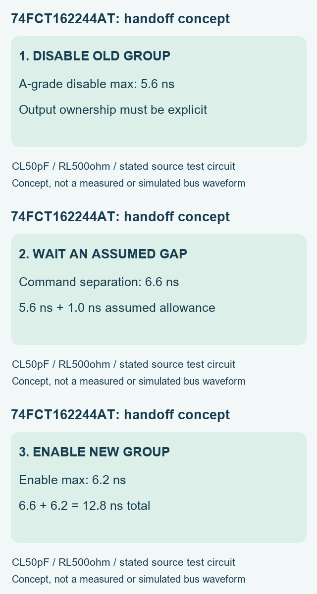
Consider a deliberately bounded handoff example with two output groups connected to a shared bus. At the first command, disable the old group. Assume a command separation of 6.6 ns before enabling the new group: the old group's 5.6 ns maximum disable time plus an explicit 1.0 ns allowance. This conservative illustration does not take credit for the new group's minimum enable delay. Its allowance is a chosen assumption, not a manufacturer-specified bus dead time or a validated clock relationship.
At the second command, the new group's maximum enable time is another 6.2 ns under the source conditions. Thus the two command-based quantities sum to 6.6 + 6.2 = 12.8 ns from the first command. This arithmetic does not establish when the receiver can sample a correct data word. Input-data stability, controller-output skew, trace delays, loading, actual high-impedance thresholds and receiver requirements remain part of the real timing review. Substituting 4.8 ns data propagation for the 5.6 ns disable limit would answer a different question and undermine the ownership schedule.
The listed 0.5 ns maximum output skew describes outputs in the same package switching in the same direction. It does not bound skew between two separately controlled devices. Likewise, the pulse-generator test rate of no more than 1 MHz on page 6 describes the test stimulus; it is not the application's maximum clock frequency. Preserve both the table and its test definitions when recording the example. A useful review asks which timing event is being bounded and where its start and end are measured.
The original animation below illustrates the three bookkeeping stages, not actual signal edges. Its static transcript is: disable the old group using its own maximum; keep a separately stated command gap; then account for the new group's enable maximum. The illustrated 6.6 ns gap and 12.8 ns total are assumptions and arithmetic, not a measured or simulated bus waveform. Read the static explanation whenever motion is unnecessary.
Play the original output-ownership concept animation
For a material-request example, suppose a board uses one 74FCT162244ATPVG at U5 and the build quantity is 25 boards. The BOM checker should return 25 devices from a per-board quantity of one. Use the sample TSV below, replacing U5 and the board count with the released design. Keep separately agreed spares explicit. The arithmetic does not establish yield, packaging multiples, MOQ, compatibility, provenance or supply. A different buffer elsewhere in the assembly remains a separate complete-MPN row.
MPN	Qty	Ref
74FCT162244ATPVG	1	U5
The handoff to purchasing should contain the exact requested number and quantity, required delivery and destination, accepted lot evidence, and the owner of any substitution decision. Keep the group-ownership and voltage/timing records with the engineering requirement. The Hard-to-find directory organizes notice evidence rather than inventory. For a board change, the PCB fabrication and assembly review routes need the real drawings and assembly scope; this article supplies no approved land pattern, thermal result or manufacturing release.
Get price and lead time for 74FCT162244ATPVG, 25 pieces. Correct the example quantity on the homepage. A sourcing request can proceed while a proposed redesign remains unapproved; keep those decisions explicit. No current stock, delivery commitment, direct replacement or human engineering certification is implied.