Lifecycle & ordering review: Literal historical replacement recommendation only. Do not inherit the affected V-code discontinuation event. Current lifecycle, lot compliance, stock, price and lead time require manufacturer/supply confirmation. Evidence and conditions ↓
Core fields reviewed 2026-11-11 Source links and conditions accompany each parameter.
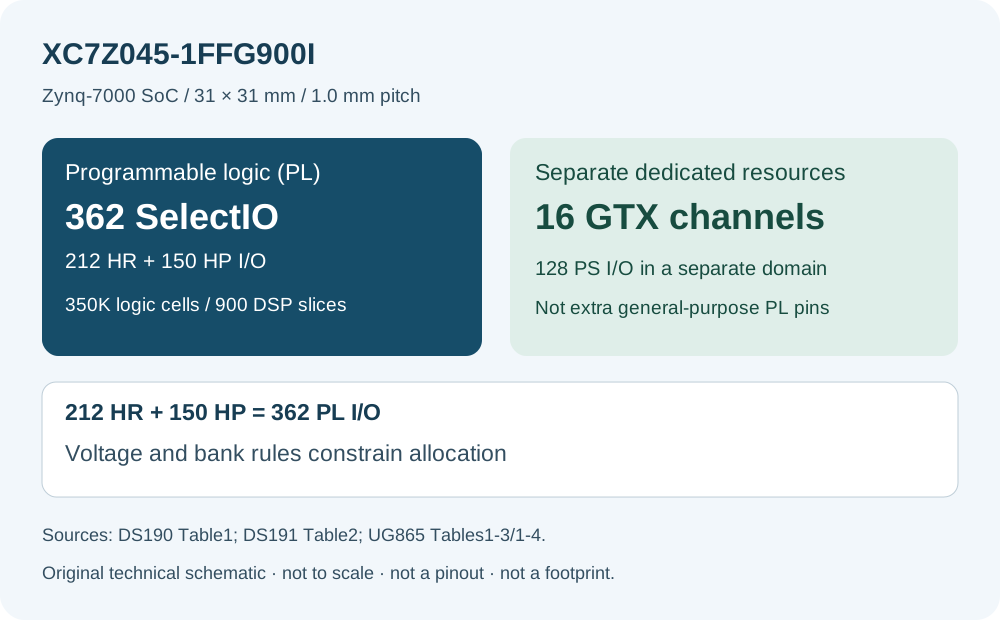
Technical schematicFFG900: 362 PL I/O / 16 GTX. 31 × 31 mm body — different ball map. Original educational schematic; calculations are hypothetical where shown. Not to scale, not a pinout, not a PCB footprint. Technical references ↗
FPGA.io Part NumberFIO-B7FCCD32F030335EInternal catalogue reference · manufacturer MPN remains unchanged
XC7Z045-1FFG900C is a system-on-chip combining an Arm processing system and FPGA programmable logic in the AMD / Xilinx Zynq-7000 SoC family, supplied in the FFG900 package. Its reviewed resources include 350,000 logic cells, 19,620 Kb of block RAM, 362 I/O for this device/package combination. This ordering code specifies speed grade -1 and Commercial (C) temperature grade. The selected device/package has 16 GTX channels; check this package-level limit before planning serial interfaces. The user-I/O figure here refers to PL SelectIO only. The 128 PS I/O in UG865 are a separate functional allocation, not interchangeable general-purpose PL pins. Use the linked manufacturer data sheets for electrical limits, pin assignments and timing. FPGA.io can review the complete part number for chip sourcing or a combined sourcing and PCBA project.
Junction temperature, not ambient. Match grade letter to DS190 p23 Figure4 and the exact XCN20011 ordering code.
Temperature grade
Commercial (C)
MPNDS190Z045 ↗p23 Table7 XC7Z045 group and Figure4; exact letter in XCN20011 p4
Core voltage conditions
0.97 to 1.03 V
gradeDS191Z045 ↗p3 Table2 VCCINT for -3/-2/-1Conditions
PL core supply, nominal 1.00 V. Do not treat as all rails. Note6 requires VCCINT and VCCBRAM connected to the same supply. PS VCCPINT has separate limits including p4 note3 CPU/DDR conditions.
Maximum application clock
Not confirmed
designConditions
Design-specific timing not established.
Application power
Not confirmed
designConditions
Workload, implementation and thermal analysis required.
Literal historical replacement recommendation only. Do not inherit the affected V-code discontinuation event. Current lifecycle, lot compliance, stock, price and lead time require manufacturer/supply confirmation.
Available stock
Not confirmed
supplyConditions
Current inventory, USD price and lead time are not verified. Request a quotation for the full ordering code.
MANUFACTURER REFERENCES
Official documents & PDF datasheets
Use the electrical data sheet together with the device overview and package/pinout information.
Full ordering-number evidence: p4 Table6, right block Replacement Part column; exact literal XC7Z045-1FFG900C. Original PDF table visually inspected..
Manufacturer documents may be revised. Verify the current revision and applicable device/package/grade before releasing a design.
DEVICE & PACKAGE DECISION
Trade the larger body for documented package resources
The FFG900 version exposes 362 PL I/O and 16 GTX channels in UG865. The same device in FFG676 exposes 250 PL I/O and eight GTX. The larger package is a physical and routing decision, not merely a different ordering suffix.
Engineering screening guidance using reviewed catalogue evidence. Examples are hypothetical and advisory; validate your actual design and the exact ordering code.
Compare body area without claiming routing density
The cited bodies are 31 × 31 mm for FFG900 and 27 × 27 mm for FFG676. Their geometric areas are 961 and 729 mm²: about 31.8% more body area. The extra 112 PL I/O is a 44.8% increase over 250, and the GTX count doubles from eight to 16. These are separate comparisons; they do not predict PCB layer count, usable routing density, thermal behavior or assembly yield. Courtyard and fan-out extend beyond body area.
What to carry into a quotation and design review
Keep XC7Z045-1FFG900C intact in the BOM and quotation. XCN20011 Table6 names this G code as a historical replacement recommendation; it does not establish current stock, current lifecycle or board compatibility. Compare the already-public XC7Z030-1FBG676C below to see the smaller XC7Z030 resource set and package-specific channels. Its 125K vendor logic cells, 400 DSP slices and 265 RAM blocks do not match this XC7Z045's 350K, 900 and 545. A similar family name cannot transfer bitstreams, pin plans, timing closure or a procurement approval. Request the exact part, quantity, grade and required date, then retain the supplier's written exceptions for review.
Result: 42 I/O remain in the count-only budget (88.4% allocated).
Planning diagram: assumed I/O allocation 320 I/O assumed allocation / 362 documented package I/O; 42 I/O unallocated. Count-only planning diagram, not a pinout or bank assignment.
88.4% of the sourced package count allocated; 42 I/O unallocated.
Each signal consumes one single-ended user I/O in this example. Dedicated serial lanes are separate. Bank voltage, differential pairing, clocks, configuration use and actual pin allocation can reduce usable capacity. Reserved signals here are an assumed design allowance, not manufacturer-reserved pins.
Result: Allocate at least 1,048,576 payload bits before adding memory overhead. The current reviewed embedded-memory reference is 19,620 Kb.
Payload arithmetic only. The source Kb/kb unit is retained; this example does not choose a decimal/binary conversion or claim a percentage fit. Round each buffer to the native memory-block geometry and check port width, depth, ECC/parity, dual-port use and implementation reports.
Public device and ordering comparisons
Compare exact package and grade conditions below. These are screening references; matching names, dimensions or resource counts do not establish pin compatibility or replacement approval.
XC7Z045-1FFG900C and already-public screening candidates
Native LUT4, LE and logic-cell metrics remain separate. Temperature is not converted to ambient; source notes define the operating basis. A family maximum is never substituted for package I/O or channels. No clock, power or stock figure is inferred.
Sources and conditions: XC7Z045-1FFG900C
Lifecycle / ordering: Literal historical replacement recommendation only. Do not inherit the affected V-code discontinuation event. Current lifecycle, lot compliance, stock, price and lead time require manufacturer/supply confirmation.
Body dimensions: 31 × 31 mm.UG865 — Zynq-7000 SoC Packaging and Pinout Product Specification · revision 1.9 · pp89–90 Figures4-13/4-14 FFG900, D and E · scope: package. Package body only, excluding PCB courtyard. For FFG900, cited lid variants share this body size; no lid variant is inferred for a supplied lot.
Core rail reference: 0.97 to 1.03 V.DS191 — Zynq-7000 SoC DC and AC Switching Characteristics (Z-7030/35/45/100) · revision 1.18.1 · p3 Table2 VCCINT for -3/-2/-1 · scope: grade. PL core supply, nominal 1.00 V. Do not treat as all rails. Note6 requires VCCINT and VCCBRAM connected to the same supply. PS VCCPINT has separate limits including p4 note3 CPU/DDR conditions.
Sources and conditions: XC7Z030-1FBG676C
Package: FFG900 → FBG676. Verify the applicable limits and design impact.
Lifecycle / ordering: Literal historical replacement recommendation only. Do not inherit the affected V-code discontinuation event. Current lifecycle, lot compliance, stock, price and lead time require manufacturer/supply confirmation.
Package user I/O: 250 I/O.UG865 — Zynq-7000 SoC Packaging and Pinout Product Specification · revision 1.9 · p11 Table1-4, XC7Z030 / FBG676 · scope: device-package. PL SelectIO only: 100 HR + 150 HP. Separate 128 PS I/O are not interchangeable PL pins. Differential counts are alternate uses, not additive.
Package dedicated channels: 4 GTX channels.UG865 — Zynq-7000 SoC Packaging and Pinout Product Specification · revision 1.9 · p10 Table1-3, XC7Z030 / FBG676 · scope: device-package. Four exposed GTX channels; not a family-maximum substitution or protocol qualification.
Logic cells (AMD): 125,000 logic cells.DS190 — Zynq-7000 SoC Data Sheet: Overview · revision 1.11.1 · p3 Table1, XC7Z030 Logic Cells row · scope: device. Source reports the rounded vendor figure 125K. This is not a LUT count.
Embedded block memory: 9,540 Kb.DS190 — Zynq-7000 SoC Data Sheet: Overview · revision 1.11.1 · p3 Table1, XC7Z030 265 × 36 Kb blocks · scope: derived. Derived capacity 265 × 36 = 9540 Kb; vendor headline is rounded 9.3 Mb. Not bytes; port geometry, parity/ECC and implementation overhead remain separate.
Core rail reference: 0.97 to 1.03 V.DS191 — Zynq-7000 SoC DC and AC Switching Characteristics (Z-7030/35/45/100) · revision 1.18.1 · p3 Table2 VCCINT for -3/-2/-1 · scope: grade. PL core supply, nominal 1.00 V. Do not treat as all rails. Note6 requires VCCINT and VCCBRAM connected to the same supply. PS VCCPINT has separate limits including p4 note3 CPU/DDR conditions.
Exact identity evidence:XCN20011 — Selected Package Product Discontinuation Notice · p4 Table6, right block Replacement Part column; exact literal XC7Z045-1FFG900C. Original PDF table visually inspected. · Historical replacement recommendation only; not an affected-device EOL assertion, current availability or compatibility approval.
Practical questions for this selection
Can an FFG676 footprint be retained for an FFG900 purchase?
No. The 900-ball and 676-ball packages have different physical arrays and documented pin maps. Recheck the PCB land pattern, bank allocation, power distribution, high-speed routing and assembly constraints before considering this package.
What does the numerical example establish for XC7Z045-1FFG900C?
It establishes arithmetic under the explicitly hypothetical inputs shown here. It is not a tool result, synthesis report, timing closure, pin-assignment validation or application qualification. Replace the assumptions with your signal list and memory geometry, then validate in the vendor tools.
For software-heavy control with limited parallel I/O, assess an MCU or processor against the same latency, interface and power requirements. For wide parallel datapaths or custom timing, compare FPGA architectures using a mapped design. For early prototyping, an evaluation board may reduce initial hardware work; verify its exact device, accessible interfaces and production suitability.
Choose what may change before comparing resources. The default keeps the same manufacturer and family, so Zynq processing-system designs are not silently matched to pure FPGAs. Same-family results still require CPU, software, pinout and timing review.
4 full MPNs meet the selected scope and numeric constraints. Showing 1 device representatives, at most two per manufacturer, ordered by smallest excess resources. Temperature, timing and pinout still require review.
Temperature grade: Commercial (C) → Industrial (I). Verify the applicable limits and design impact.
Numeric matches do not establish pin compatibility, protocol support, lifecycle or supply availability.
Numeric screening is not replacement approval.
Logic and DSP mapping, pinout, bank voltages, temperature, timing, protocol support and toolchain remain engineering checks. Serial channel quantity does not verify data rate or protocol support. Cross-brand candidates generally require board and HDL review.
Closest documented device and package variants appear first. Package, grade and pinout may differ; these are comparison candidates, not approved replacements.