Memory-interface chipsets is a product-line reference within Rambus. Use the manufacturer source to confirm the exact device or deliverable and its current support status.
Chips & IP: distinguish a packaged device requirement from an IP integration project.
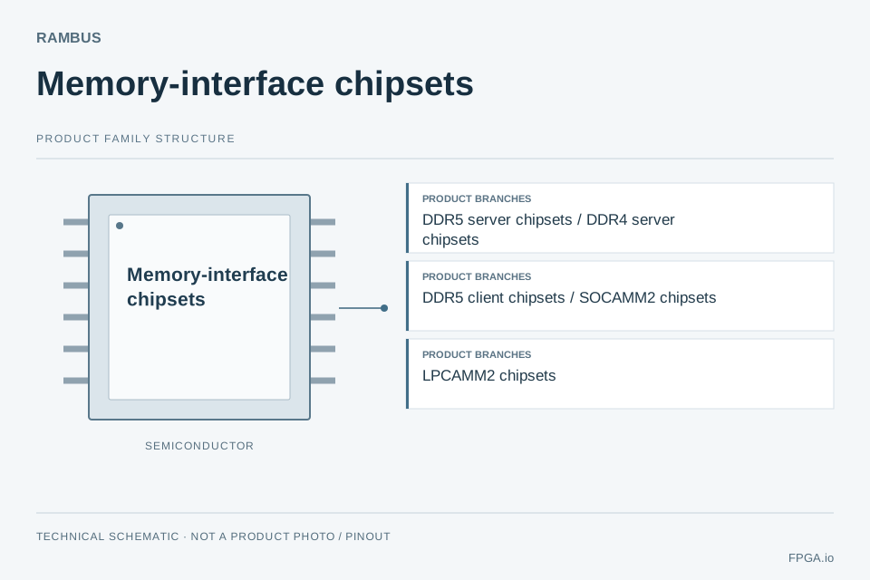
Technical schematicFPGA.io technical schematic for Memory-interface chipsets. Product branches are shown as a navigation overview. This is an abstract diagram, not a product photograph, package drawing or pinout. Technical reference ↗
This category map is being expanded. Linked device examples have individual sources; they do not represent the complete manufacturer catalogue.
Define the integration scope
Chips & IP: distinguish a packaged device requirement from an IP integration project.
Confirm the protocol revision, data rate, logic level, channel count and termination requirements.
Review signal integrity, isolation where applicable, clocking and package pinout before substitution.
Confirm licensing, target process or host architecture, integration deliverables and verification responsibilities.
An IP licence is not a packaged IC; distinguish design-service, licence and silicon procurement scopes.
Define key provisioning, secure boot, authentication interface and lifecycle/ownership requirements.
Chips & IP: distinguish a packaged device requirement from an IP integration project. This page describes Chips & IP. Chip relationships are shown only when explicitly documented; a same-brand reference does not establish tool support or board compatibility.
Documented device references
Base-device names are distinct from full ordering numbers. Each detail page identifies the product type, parameter scope and official source.
DDR5 server chipsets is a rambus product family or category shown in the manufacturer product navigation. Select the exact device from the manufacturer table.
DDR4 server chipsets is a rambus product family or category shown in the manufacturer product navigation. Select the exact device from the manufacturer table.
DDR5 client chipsets is a rambus product family or category shown in the manufacturer product navigation. Select the exact device from the manufacturer table.
SOCAMM2 chipsets is a rambus product family or category shown in the manufacturer product navigation. Select the exact device from the manufacturer table.
LPCAMM2 chipsets is a rambus product family or category shown in the manufacturer product navigation. Select the exact device from the manufacturer table.
Manufacturer or identified public portfolio reference.
These broader manufacturer resources do not establish support or compatibility for every device on this page.
PRACTICAL QUESTIONS
Memory-interface chipsets selection questions
Which product or release should I specify?
Use the exact product name and revision, together with the target device and intended workflow. Memory-interface chipsets is a product-line reference within Rambus. Use the manufacturer source to confirm the exact device or deliverable and its current support status.
How do I check device support?
Use the manufacturer support matrix, release notes or board documentation for the exact revision. Record the exact target device and version; a shared manufacturer alone does not prove compatibility.
What should be checked before integration?
Chips & IP: distinguish a packaged device requirement from an IP integration project. Identify the required IP configuration, supported process or platform, interfaces and integration deliverables.
What should I include in a project request?
Describe the application, exact product or revision, target hardware, quantities and delivery requirements. State which components, board manufacturing, programming and test work you need reviewed.
PREPARE A USEFUL INQUIRY
Build your selection brief.
Select the points you want our team to review. Your selections stay in this browser until you choose to submit the quotation form.