
Hard-to-find
ispPAC-CLK5304S-01T48I: Reconstruct Two Clock Banks Before Replacing a Legacy Board Part
Published · Updated
Use this guide when a service board calls for ispPAC-CLK5304S-01T48I and you have its schematic, clock list or a retained programming file. The decision is whether the required clocks fit two shared electrical banks and whether the archived PLL configuration can be reconstructed. It keeps the exact conventional order code and the historical lead-free replacement separate until the repair team has enough evidence to accept a change.
Request exact ispPAC-CLK5304S-01T48I · edit quantity on the homepage
Reconcile the conventional and lead-free records
The ispClock5300S data sheet, DS1010 revision 01.4, lists the complete industrial conventional order on PDF page 49. The exact line is ispPAC-CLK5304S-01T48I, with four clock outputs, a nominal 3.3 V supply, 48 pins and TQFP packaging. The ordering key identifies 01 as the standard performance designation, T48 as the conventional package code and I as industrial. The following page lists ispPAC-CLK5304S-01TN48I in the lead-free group. Preserve the complete letter sequence in the service record.
The manufacturer discontinuation notice and its attached affected workbook address the conventional order. In AffectedOPNs_All, row 3 column C contains the exact T48I and the alternative column names TN48I. The row sits in Group 1 for selective SnPb withdrawals. Its historical compatibility fields record availability, pinout, voltage and SnPb assembly compatibility as yes under the terms of that notice. Carry those as dated manufacturer statements about the listed codes. A current offer still requires its own evidence, and the old sheet cannot qualify the lot or the repaired assembly.
The notice is dated 2015-06-23 and records 2015-12-23 as last-time-buy and 2016-12-30 as last shipment under the historical terms. Keep those dates distinct from the October 2007 revision date of the data sheet. The latter identifies the technical document, while the notice and row identify the later procurement event. Neither document gives a supplier's present stock, condition or shipping promise.
Use the exact-device guide to log the exact requested code, the exact offered code and the evidence for each. Attach the actual marking photo or label record if the seller provides one. Ask which assembly revision the offer is meant to repair. A lead-free part may be the intended alternative on one service revision while a different repair instruction requires the original finish or retained device configuration.
Assign outputs by electrical bank before counting them
PDF pages 24 and 25 describe two output banks in the 5304S, with two outputs in each bank. The A and B outputs of a bank share a logic standard and the bank's VCCO supply. A different bank can support a different documented standard with the corresponding rail and conditions. Individual output settings such as slew, polarity and enable still need review. Four physical clock outputs therefore do not give four independent voltage domains.
Start with a table containing endpoint, required clock frequency, input logic standard, endpoint loading, startup requirement and board route. In a hypothetical design using internal PLL feedback, two 3.3 V LVCMOS receivers use the two outputs of one bank and two 1.8 V LVCMOS receivers use the other. This is an allocation starting point. Check the supply and output tables for each standard, whether the actual wiring places both members on the intended bank, and whether the loads fit the assumed output behavior.
A third required output standard changes the result even if the total output count remains within four. For example, three receivers may separately require 3.3 V LVCMOS, 2.5 V LVCMOS and 1.8 V LVCMOS. Their standards require three bank groups in this simple direct-drive plan. Two groups are available. Changing one receiver's permitted standard, adding an external interface stage or redesigning the clock tree all require their own evidence and verification.
Document the supply at each bank alongside its chosen logic standard. The power rails worksheet can organize known voltage, current and efficiency assumptions. Use a separate row for each relevant rail and leave unavailable current values open until measured or estimated from the applicable conditions. The rail worksheet does not establish output edge quality, receiver thresholds or the power-up behavior of the clock tree.
Rebuild the divider plan for the actual operating mode
PDF pages 18 and 19 show three programmable V dividers with legal divisors of 1, 2, 4, 8, 16 and 32. With the PLL selected and locked, equation 1 gives the output rate as reference rate multiplied by the feedback divider and divided by the chosen output divider. The document's VCO table gives 160 to 400 MHz. Check the selected reference and feedback limits, the skew mode and the output rate limits as separate constraints.
Consider an explicitly hypothetical locked example using a 50 MHz reference and feedback divisor four. The corresponding arithmetic gives 200 MHz for the VCO. An output divisor of two yields 100 MHz and an output divisor of four yields 50 MHz. Put those two frequencies in the worksheet beside the intended output bank assignments. They are candidate arithmetic results, conditional on the selected PLL and configuration, their legal ranges and the actual retained clock tree.
In bypass mode the reference routes directly to the divider chain. Equation 2 gives reference rate divided by the output divisor. In the same arithmetic example, a divide-by-two output becomes 25 MHz and a divide-by-four output becomes 12.5 MHz. Page 19 says the lock-detect and skew-generation functions are unavailable in bypass and documents the inverted output for a divide-by-one setting. Keep the bypass settings and expected startup behavior in a separate column.
The 50 MHz example must not inherit the jitter figures on page 11 that are conditioned on phase-detector input of at least 100 MHz. Confirm the applicable observation bandwidth, signal standard, mode and load when planning a measurement. Page 19 also distinguishes internal and external feedback. Internal feedback leaves all four outputs available for distribution. With external feedback, identify the output that closes the loop before counting the outputs available for distribution. If a receiver shares that output, verify the receiver loading and the feedback route. For an external loop, use the trace delay worksheet to estimate a board contribution separately. A hypothetical 45 mm route at 150 mm/ns gives 0.3 ns one way. That scalar number does not establish loop delay, skew at the receiver or phase margin.
Preserve the source and settings that select the feedback path. A net called feedback in a schematic and a divider called feedback in a programming file describe different pieces of the implementation. Check which output is returned, which divider closes the loop and whether the reference selection matches the board strap. If the programming data are missing, record the expected output and the uncertainty before attempting to match an offered part.
Record the reference, feedback and output divisors as separate fields even when two values happen to be equal. A frequency list without those fields cannot explain why the measured clock changes when the device enters bypass. For a practical repair record, make one row for expected operation after lock and another row for the temporary startup mode. State whether the receiver may start before the clock is stable, who owns that decision, and where on the board the expected frequency will be checked.
| Mode | Input to output dividers | Divide by two | Divide by four |
|---|---|---|---|
| PLL locked | Assumed 200 MHz VCO | 100 MHz | 50 MHz |
| Bypass | Assumed 50 MHz reference | 25 MHz | 12.5 MHz |
Play the three-step clock-bank and divider concept
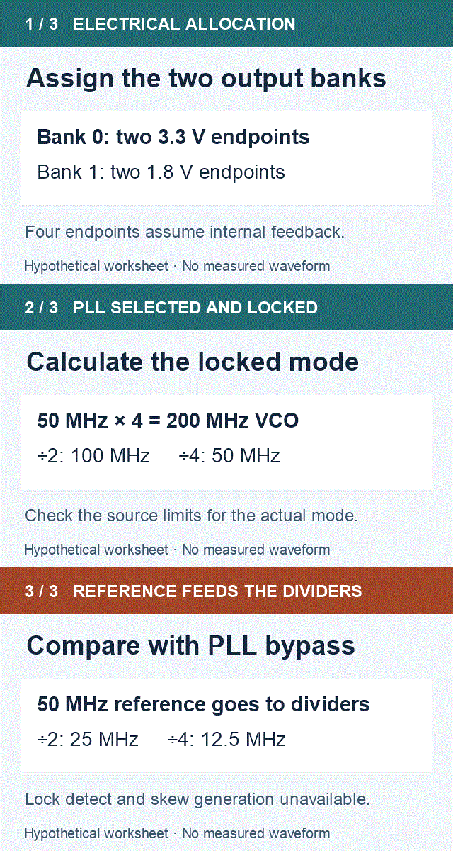
- For the four-endpoint example, assume internal feedback. Group endpoints by required output standard. With external feedback, account for the output used to close the loop.
- For an assumed locked mode with 50 MHz reference and feedback divisor four, calculate a 200 MHz VCO and 100 MHz and 50 MHz divider outputs.
- For bypass and the same output divisors, calculate 25 MHz and 12.5 MHz. Lock detect and programmable skew generation are unavailable in bypass.
Use the 5304S lead column and inspect control states
The data sheet combines the 5304S, 5308S and 5312S in one pin table. Read the 5304S column on pages 42 and 43. On this exact 48-lead option, bank zero has VCCO at 5, outputs at 6 and 8, and ground at 7. Bank one has VCCO at 32, outputs at 31 and 29, and ground at 30. The same lead numbers on a larger sibling cannot be assumed to carry those functions.
The source table accounts for all 48 positions, including sixteen no-connects. For the functional review, keep the reference pins at 14 and 15, feedback input at 17, reference selection at 19, reset at 20, lock indication at 45 and bypass control at 44 visible alongside the output assignments. Keep analog supply and ground, digital supply and ground, output-bank rails and JTAG I/O supply as distinct named nets in the review.
Page 51 provides a top view for the 5304S 48-pin TQFP, with an example commercial marking on that diagram. Use the exact industrial ordering row for temperature and ordering identity. The archive package drawings include more than one 48-pin TQFP outline and do not establish which thickness belongs to this exact offered lot. Obtain the applicable drawing and assembly evidence before using the source pin diagram as a production footprint or clearance approval.
The service procedure should check which reference input is selected, which mode straps are active at startup and when outputs may enable. Capture the actual control values, expected rail ramp, board revision and receiver tolerance. Keep the intended design state separate from a state observed on a failing assembly. The PCB bring-up checklist can organize those observations and prevent a missing image or wrong strap from being mistaken for a bad part.
Keep the temperature basis and the rail limits explicit
Page 5 gives recommended core and analog supplies of 3.0 to 3.6 V. The JTAG I/O supply range is listed separately as 1.62 to 3.6 V, and the output-bank rail depends on the programmed standard. Record actual voltages at the applicable pins across load and startup. The ordering table's nominal 3.3 V is a part description and does not set every rail or termination input to that voltage.
For industrial operation, page 5 lists ambient temperature from minus 40 to plus 85 °C and operating junction temperature from minus 40 to plus 130 °C. The ambient row has a footnote about the effect of device dissipation on its upper limit. Carry both terms, the power estimate and the enclosure or board conditions into a thermal review. A rail or ambient label on a BOM is not an approved thermal measurement.
Review output levels against the receiving threshold, and review each receiver's load separately. An output bank can have the correct nominal standard while its actual amplitude or rise time at the receiver fails an application requirement. The source output impedance settings and reference termination options can guide a bench plan. The actual stack-up, trace length, connector, endpoint and measurement method still define the conditions under which the result is useful.
The critical records are the released configuration, intended clock input, required output mode, board wiring and measured behavior. Record a test sequence that first checks power and reference, then inspects reset, bypass and the expected lock behavior for the chosen mode, and finally verifies the signal at its endpoint. Treat an unresolved configuration file or unknown programming state as a condition to resolve before accepting the repair.
Prepare the exact request and the acceptance checks
If the service decision is to retain the exact conventional part, request ispPAC-CLK5304S-01T48I and the actual number of required devices. In the BOM checker, a simple example of twenty-five boards with one clock device each yields twenty-five units. Enter separate quantities for any spares or inspection samples. Preserve the complete order code when combining the purchase request with a service work order.
If the repair team wants to consider the historical TN48I alternative, keep that proposal on its own line with the notice reference, lot documentation, lead finish and manufacturing acceptance conditions. Require a matching configuration record, rail and output-standard checks, and a verified bring-up path. If the proposed offer cannot be tied to the required code or programming state, leave the decision open for the buyer and responsible engineer.
Request traceable marking and lot evidence without assuming that a catalogue image describes the actual offer. The archived notice explains a past change and gives a starting point for comparing codes. It does not resolve current storage history, solderability, device programming state, stock, price or delivery. Record the date and source for any facts the seller confirms so a later review can distinguish those from the manufacturer archive.
The useful output is a written clock assignment and a separate sourcing line. Include the bank standards, expected frequencies for the selected mode, named control states, required observations and actual quantity. Use the Hard-to-find directory to return to the lifecycle evidence when the purchase or engineering record needs to be checked.
For the output review, include two separate sets of acceptance notes. One set belongs to the device and board configuration, including the output assignment and the intended reference behavior. The other belongs to the offered units, including the package marking, the order code and any programming evidence the seller can document. Keep the notes tied to the same board revision so the approval record remains useful after the next component substitution proposal.
Keep the requested and offered clock codes separate
Create a downloadable review record before preparing an inquiry. For the example above, enter Lattice, requested ispPAC-CLK5304S-01T48I, the full code actually offered, and 25 components. An offered ispPAC-CLK5304S-01TN48I must remain a different ordering string. Mark evidence checked only after consulting the actual source and recording its revision and page or workbook row. A matching string does not approve the lot, configuration or board.
Inputs are processed in this page only. The inquiry link opens the requested code and quantity; it does not send a request.
Enable JavaScript for the worksheet, or use the static checklist below.
Static checklist and no-script fallback
Record manufacturer, requested full MPN, offered full MPN, component quantity, and the exact evidence reference. Preserve T48I and TN48I as different codes. Leave source evidence unresolved if its revision or row has not been checked. Keep package, lead finish, programming state and board acceptance open for the responsible buyer and engineer.
MPN	Qty	Ref
ispPAC-CLK5304S-01T48I	1	U1
Enter the actual quantity for ispPAC-CLK5304S-01T48I
This guide was prepared with AI assistance. The source evidence and manuscript received independent AI review; this is not human engineering certification. The examples describe planning arithmetic and archive evidence.