
Hard-to-find
74FCT20807PYGI: Keep 150 ps Out of the Wrong Clock Budget
Published · Updated
74FCT20807PYGI is an obsolete one-to-ten clock driver whose 150 ps skew number belongs to a defined comparison, not an entire board. This guide helps a legacy-system buyer preserve the exact request while separating fanout, test load, receiver conditions and a historical redesign suggestion.
It reads the May 2010 DSC-6171/14 datasheet, the PLC250016 notice and the manufacturer’s exact product records. All calculation examples are hypothetical; no offered lot, board, clock tree or present supply is qualified.
Request price and lead time for 74FCT20807PYGI, 25 pieces on the homepage. Set your actual required quantity. Availability, price, delivery and any proposed alternate need confirmation.
Read the exact withdrawal before interpreting a suggested replacement
The exact number 74FCT20807PYGI names the industrial, tube-carried SSOP version of a two-and-a-half-volt clock-distribution component. The exact manufacturer product page identifies it as obsolete, with twenty leads, package code PYG20 and ten outputs from one input. These fields help match a request to its documentation. They do not authenticate an offered lot, establish usable stock, or confirm that an installed board will work after a component change.
PLC250016, issued on 30 May 2025, lists this exact number on page 3 in the affected-part column. Its last-time-buy date is 30 November 2025 (2025-11-30), and its last-shipment date is 30 May 2026 (2026-05-30). The current download was compared with the retained earlier copy and has identical bytes. Reading it again does not make those historical factory milestones current quotation terms, and the document retrieval date must remain separate from the notice issue date.
The same row places 5PB1106PGGI in a column headed Replacement/Similar/Re-Design. That column is deliberately broader than a compatibility approval. The suggested part is a six-output device in a fourteen-lead TSSOP, while the requested part has ten outputs in a twenty-lead SSOP. Even before checking thresholds or timing, a buyer has a concrete reason to stop an automatic one-line substitution and ask what the maintained clock tree actually needs.
Preserve the original number, the proposed number and the review decision as separate fields. A newer component with an attractive jitter headline cannot silently inherit the original fanout, board connections or startup behavior. The notice requests work with the manufacturer to determine suitable replacements; it does not supply a released schematic change, firmware change or manufacturing approval. The useful output here is a reviewable difference record, rather than an assertion that the historical suggestion is wrong or ready to install.
The complete-ordering-number tutorial explains the general identity workflow. For this device, add the number of clock receivers and the board revision before asking for an alternate. Keep the tube code distinct from the separately listed reel suffix. A purchasing line can be perfectly literal while still missing the circuit requirements that determine whether a different clock driver could be evaluated at all.
Account for ten clock outputs and every supply connection
The functional diagram on page 1 of the May 2010 datasheet shows one input feeding ten non-inverting clock outputs. This is a distribution function, not a phase-locked loop, frequency synthesizer or general bidirectional data-bus transceiver. It does not multiply a clock frequency or recover a missing reference. A board review should identify which source drives the input, which receivers use the outputs, and which clock relationships matter to those receivers.
The top-view connection diagram has one input, ten output positions, four VCC positions and five ground positions. Their sum is twenty. Multiple supply and ground leads are part of the noise-control arrangement; they are not spare outputs that can be reassigned. The source places the input at pin 1 and supply at pin 20, but an actual released symbol must be checked against the entire diagram and board orientation. This guide does not provide a CAD library or a continuity-test result.
Give each used output a receiver name, the receiver input standard, a loading assumption and a physical route. Mark an unused output explicitly, rather than reducing the documented fanout to whatever happens to appear in an incomplete BOM. Ten available outputs do not prove that all can drive arbitrary connector loads at the headline frequency. Conversely, a design using only six outputs still needs the positions and behavior checked before a six-output replacement is considered.
The exact product page links PYG20 to an SSOP package and lists a nominal pitch of 0.65 mm with catalogue dimensions of 7.2 by 5.3 by 1.73 mm. The PYG20 package page confirms the package identity. These are useful catalogue descriptors, but a current complete tolerance drawing, land pattern and board-clearance review were not obtained in this check. An active package record also does not reverse the obsolete status of a specific component that used that package.
The published sixteen-bit three-state buffer guide provides a relevant functional contrast. Its enable groups and five-volt bus handoff do not describe this one-to-ten clock driver. Similar letters in a part family are not a reason to reuse its control assumptions. For an assembly review, retain the exact SSOP identity and request the released original component and board documents; a sourcing article is not a footprint or process qualification.
Keep the operating range separate from stress and receiver limits
The DC operating table on page 3 defines industrial operation using ambient temperature, TA, from minus forty to plus eighty-five degrees Celsius, with VCC at 2.5 V plus or minus 0.2 V. That is a 2.3 V to 2.7 V operating-supply range. This ambient definition must not be replaced with a junction-temperature range from an FPGA article or another clock family. Board thermal behavior and the actual environment still require their own assessment.
The same table gives a minimum input-high level of 1.7 V and a maximum input-low level of 0.7 V. Those are input recognition limits under the stated scope, not a statement that any clock amplitude or any powered-off interface is safe. The absolute-maximum table on page 2 is a separate stress table. Its input-terminal limit must not be reused as a normal operating target or as permission for arbitrary five-volt clock operation.
Output voltage guarantees depend on output current. At the specified minimum supply, the light-load high-level guarantee is VCC minus 0.2 V at minus 1 mA. The heavier-load row prints 1.8 V at minus 8 mA, while footnote 5 says VCC minus 0.6 V. At the minimum supply those statements must not be silently resolved into a new guaranteed margin; clarify the combination before relying on it. The low-level rows likewise have separate one-milliamp and eight-milliamp conditions. A correct interface review compares the appropriate guaranteed output level with the actual receiver threshold and load, rather than comparing two nominal voltage labels.
The current product page calls the input and output LVCMOS, while the older document also uses TTL-compatible wording. Treat those descriptions as pointers to the numerical DC and switching conditions, not as a universal interface approval. If a receiver is a particular FPGA bank, its configured input standard, bank supply, reference requirements and absolute limits must be read from that exact FPGA documentation. No receiver has been electrically qualified by this article.
The power-rail planning tool can organize explicit assumptions, but it does not create a regulator specification from typical current. Page 2 separates quiescent current, input-related current and dynamic current under particular loads and frequencies. A typical headline must not replace a worst-case rail budget. Record the chosen source row and unresolved loading before a quotation is used to justify a board change or a power-supply decision.
| Field | Source value | Condition and locator |
|---|---|---|
| Exact identity | 74FCT20807PYGI | PLC250016p 3; exact product page |
| Operating supply | 2.3–2.7 V | VCC2.5 V±0.2; DSpp 3–4 |
| Industrial temperature | TA−40..+85°C | Ambient definition; DSpp 3–4 |
| Clock fanout | 1 input / 10 outputs | Functional and 20-lead diagram; DSp 1 |
| Propagation maximum | 3.5 ns or 2.7 ns | 22pF100 MHz or 12pF150 MHz; DSp 4 |
| Same-device skew maximum | 150 ps | Identical transitions and loads; DSp 4note 4 |
| Part-to-part skew maximum | 600 ps | Identical transitions/load/VCC/TA; DSp 4note 6 |
Carry the test load with every propagation-delay number
The cover feature list describes high-speed propagation below three nanoseconds. The detailed switching table on page 4 shows why the surrounding conditions are essential. At a load of 22 pF and 100 MHz, it lists a typical propagation delay of 3 ns and a maximum of 3.5 ns. At 12 pF and 150 MHz, it lists 2.4 ns typical and 2.7 ns maximum. A reader cannot select the smaller number while keeping the larger load and call that the guaranteed original specification.
Both rows are within the listed industrial ambient-temperature and supply range. Page 5 defines load capacitance as including fixture and probe capacitance, and its timing sketches use a 1.25 V crossing reference. Output rise and fall are measured between the marked voltage levels; they are not simply a whole clock period divided by an arbitrary ratio. A real measurement must document probe loading and reference levels before it can be compared with those rows.
The footnotes distinguish production-tested propagation delays from the other parameters that are guaranteed but not production tested. Keep that manufacturer distinction intact. It does not mean that FPGA.io performed a timing test, nor does it turn a data-sheet guarantee into a measured value for an offered lot. Record whether the evidence is a published specification, a project calculation, a simulation or a real test log, and do not substitute one category for another.
For frequencies above 133 MHz, the source recommends airflow of one metre per second. That recommendation belongs with the high-frequency use case; it must not disappear when quoting the 150 MHz row. The table is still not a system clock-closure report. Actual supply noise, duty cycle, receiver loading, routing and enclosure conditions can matter even when the nominal frequency fits a published headline. Their remaining validation should be visible in the handoff.
Build a comparison record with load, frequency, supply, ambient scope, typical or maximum category, timing threshold and the parameter name. If one of those inputs is unknown, leave the comparison unresolved. Do not infer a minimum propagation bound from a blank minimum cell. A maximum delay alone cannot supply every side of a setup-and-hold calculation, and the source explicitly says its propagation-delay range does not itself imply skew.
Use the right skew category before adding a route estimate
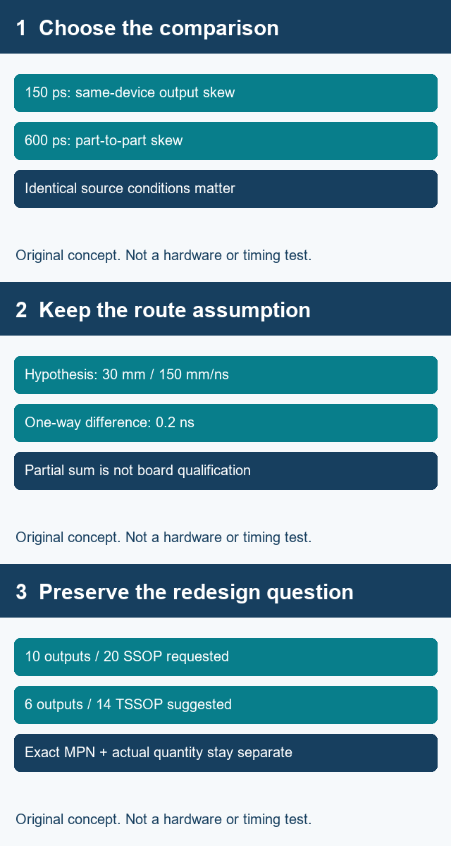
The same-device output-to-output skew maximum is 150 ps under identical transitions and load conditions. Pulse skew has a separate 300 ps maximum, describing the difference between rising and falling propagation on one output. Part-to-part skew has a 600 ps maximum, with identical transitions, loads, supply levels and temperature. These parameters answer different questions. A pair of receivers driven from different chips cannot inherit the single-chip 150 ps figure simply because both drivers carry the same ordering number.
Page 5 illustrates those categories separately. It also limits the part-to-part example to the same package type and speed grade. None of these figures is a universal end-to-end board skew, and a picosecond skew limit is not an RMS phase-jitter value. Preserve the parameter identity and the correlated conditions before adding board effects. Taking a convenient headline from a proposed replacement without its measurement scope would produce a misleading comparison.
For a deliberately hypothetical route example, assume two relevant paths differ by 30 mm and use an assumed propagation velocity of 150 mm/ns. Enter 30 for trace length and 150 for velocity in the trace propagation estimate. The output should be 0.2 ns, or 200 ps. Here the supplied length represents only the path-length difference; the calculator itself performs scalar one-way length divided by velocity, not a clock-tree analysis.
Adding the original single-device 150 ps value to that hypothetical 200 ps route difference gives 350 ps, or 0.35 ns, as a deliberately incomplete planning sum. It is not a new guaranteed skew specification. The arithmetic excludes actual stack-up variation, unequal loads, vias, discontinuities, driver and receiver thresholds, jitter, correlation and other timing terms. It also assumes that the selected same-device category and source conditions apply, which a real design must establish independently.
Use the example to ask which evidence is missing, rather than to approve a timing margin. If the routes come from different devices, or the loads are not identical, start again with the appropriate category and documented conditions. A tighter trace match cannot automatically repair an unsupported driver comparison. Conversely, a positive arithmetic remainder cannot establish setup-and-hold margin without the actual launching and receiving requirements and clock relationships.
The useful deliverable is a small clock-path record: source, output and receiver identity; chosen skew category; stated load and voltage conditions; route assumption; and items still outside the model. Clear an input in the calculator and confirm that the old result becomes invalid. Unknown length or velocity must not become zero delay. Save the assumptions alongside the output so that another reviewer can reproduce the limited calculation and reject an inapplicable use.
Treat the six-output suggestion as a redesign question and preserve the inquiry
The current manufacturer page for the historically suggested 5PB1106PGGI identifies a one-to-six LVCMOS clock buffer. Its current 5PB11xx datasheet, dated 22 September 2026, lists that exact tube-carried industrial code on page 22 in a fourteen-pin TSSOP. This is positive evidence of a topology and package difference from the requested one-to-ten, twenty-pin SSOP. It is enough to prevent an automatic substitution; it is not a complete qualification of the suggested part.
Do not replace ten original outputs with six and assume that the remaining four were unused. Even a maintained board that uses only six clock destinations needs an explicit pin, supply, loading, enable and startup review. A different footprint or added enable function can change both board work and behavior. The historical notice does not provide those decisions. The currently suggested device is discussed here only to explain the review boundary, not as an approved purchase recommendation.
Keep an exact-part sourcing request separate from an authorized redesign study. The former needs the complete original number, required quantity, offered-lot evidence and any agreed inspection or test conditions. The latter needs the released schematic, actual clock destinations, board revision, receiver requirements and a reviewable change plan. Those paths may share documents but should not share an unqualified approved checkbox. Private board files also belong outside public query strings.
For a hypothetical twenty-five-board build with one 74FCT20807PYGI at UCLK1, paste the example row into the BOM checker and enter 25 boards. The expected arithmetic output is 25 components before any separately entered spare, loss, order-minimum or pack-rounding assumptions. The original tube carrier does not by itself impose a quantity of 64 on your engineering requirement. Preserve the user quantity rather than silently rounding it to a catalogue carrier count.
Return through the Hard-to-find directory when comparing historical evidence with other reviewed exact-model routes. An offered component still needs provenance, condition and delivery review, while a redesign still needs engineering and manufacturing validation. This article supplies source-linked questions and reproducible planning arithmetic. It does not establish present inventory, price, lead time, a successful boot or a qualified clock replacement. The homepage inquiry preserves the exact requested number and quantity so those open questions can be addressed explicitly.
MPN	Qty	Ref
74FCT20807PYGI	1	UCLK1
The original animation is a conceptual review sequence: identify the skew category, retain the load and routing assumptions, then preserve the exact sourcing or redesign question. It is not a measured waveform, a simulation trace or a timing-closure result. This static explanation remains visible when the animation is hidden.
Play the original clock-budget concept
Get price and lead time for 74FCT20807PYGI, 25 pieces. Preserve the exact number, actual quantity and any requested traceability or test conditions. This opens a reviewable request, with no inventory or engineering approval implied.
Prepared with AI-assisted manufacturer-document analysis. A separate AI source, full-text and visual review was completed before release. No human engineering sign-off, simulation run or hardware test is represented.