
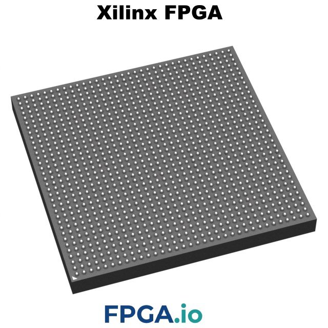

Description
XCZU49DR-2FFVF1760I Overview
The XCZU49DR-2FFVF1760I is an AMD (Xilinx) Zynq® UltraScale+™ RFSoC Gen 3 device built on 16 nm FinFET+ technology. It integrates a 64-bit quad-core Arm® Cortex®-A53 application processor, a dual-core Arm Cortex-R5F real-time processor, UltraScale+ programmable logic, and a complete direct-RF-sampling data converter subsystem on a single die.
Within the RFSoC family, the ZU49DR is the highest-channel-count member: 16 RF-ADCs and 16 RF-DACs (16T16R) in one package. That makes XCZU49DR-2FFVF1760I the natural choice for dense multi-channel systems — digital phased-array radar, massive-MIMO radio heads, wideband electronic warfare receivers and multi-beam satellite payloads — where channel density per board, not per-channel sample rate, is the binding constraint.
Key Technical Highlights
- Direct RF sampling to 6 GHz — no external mixer chain required for sub-6 GHz bands.
- 16× 14-bit RF-ADC, up to 2.5 GSPS each, arranged as four quad-ADC tiles with one PLL per tile. Each RF-ADC includes a digital down converter (DDC) with a 48-bit NCO, full complex mixer and programmable decimation (1x through 40x).
- 16× 14-bit RF-DAC, up to 9.85 GSPS each, in four quad-DAC tiles, each with a digital up converter (DUC), 48-bit NCO, sin(x)/x correction and 1st/2nd Nyquist zone support. 4 GHz full-power output bandwidth, RF output to 5 GHz.
- Multi-chip synchronisation and on-chip clock forwarding (a Gen 3 feature) for deterministic phase alignment across tiles and across devices — essential for beamforming arrays.
- Quadrature modulator correction (gain / phase / offset) per converter pair, plus programmable amplitude threshold flags per RF-ADC.
XCZU49DR-2FFVF1760I Full Specifications
RF Data Converter Subsystem
| RF-ADC channels | 16 × 14-bit, up to 2.5 GSPS (4 quad tiles) |
| RF-DAC channels | 16 × 14-bit, up to 9.85 GSPS (4 quad tiles) |
| Max RF input frequency | 6 GHz |
| DDC / DUC | Integrated per converter, 48-bit NCO, dual-band capable |
| Decimation / interpolation | 1x, 2x, 3x, 4x, 5x, 6x, 8x, 10x, 12x, 16x, 20x, 24x, 40x |
| SD-FEC blocks | 0 (see note below) |
Processing System (PS)
| Application Processing Unit | Quad-core Arm Cortex-A53 MPCore w/ CoreSight, NEON, SP/DP FPU, up to 1.3 GHz |
| L1 / L2 cache | 32 KB + 32 KB per core / 1 MB unified L2 with ECC |
| Real-Time Processing Unit | Dual-core Arm Cortex-R5F w/ CoreSight, up to 533 MHz, TCM with ECC |
| On-chip memory | 256 KB OCM with ECC |
| DDR controller | DDR4 / DDR3 / DDR3L / LPDDR4 / LPDDR3, up to 2400 Mb/s, 32/64-bit, optional ECC, up to 32 GB |
| PS peripherals | 4× Gigabit Ethernet (IEEE 1588v2), 2× USB 3.0/2.0, SATA 3.1, DisplayPort 1.2a, Quad-SPI, NAND (ONFI 3.1), SD/eMMC 4.51, 2× UART / SPI / I2C / CAN 2.0B, up to 128b GPIO, RTC, WDT |
| Security | CSU with 256-bit AES-GCM, SHA-3/384, 4096-bit RSA, TrustZone, secure boot |
Programmable Logic (PL)
| System logic cells | 930,300 |
| CLB LUTs | 425,280 |
| CLB flip-flops | 850,560 |
| Block RAM | 38.0 Mb (1,080 × 36 Kb blocks, with FIFO + ECC) |
| UltraRAM | 22.5 Mb (80 blocks, 4K × 72) |
| Distributed RAM | 13.0 Mb |
| DSP slices | 4,272 (27 × 18 multiplier, 48-bit accumulator, 96-bit XOR, pre-adder) |
| Clock management tiles (CMT) | 8 · Fractional PLLs: 8 |
| System Monitor | 2 (PL: 10-bit 200 kSPS · PS: 10-bit 1 MSPS) |
Connectivity & I/O
| GTY transceivers | 16, up to 28.21 Gb/s per lane (speed grade -2) |
| PS-GTR transceivers | 4, up to 6.0 Gb/s |
| PCI Express | 2× integrated PCIE4C blocks — Gen3 x16 or Gen4 x8, CCIX 1.0 capable, Endpoint or Root Port |
| 100G Ethernet | 2× 100G MAC/PCS with RS-FEC (IEEE 802.3ba / 802.3bj), CAUI-4 and CAUI-10 |
| Interlaken | 1× 150G integrated block (1–12 lanes) |
| User I/O | 622 total — 312 HP I/O + 96 HD I/O + 214 PS I/O |
Package, Grade & Environmental
| Manufacturer part number | XCZU49DR-2FFVF1760I |
| Manufacturer | AMD (Xilinx) |
| Package | FFVF1760 — 1760-ball FCBGA, lidded flip-chip |
| Body size / ball pitch | 42.5 × 42.5 mm / 1.0 mm |
| Speed grade | -2 |
| Temperature grade | Industrial (I), -40°C to +100°C junction |
| VCCINT | 0.85 V |
| Process | 16 nm FinFET+ |
| RoHS | Compliant (V = RoHS 6/6) |
| Packaging | Tray |
Part Number Decoder: XCZU49DR-2FFVF1760I
- XC — Xilinx commercial product
- ZU — Zynq UltraScale+ architecture
- 49 — value index (device size / converter configuration)
- D — processing system: quad APU + dual RPU
- R — engine type: RF Signal (RFSoC)
- -2 — mid speed grade
- F — lidded flip-chip package (S = lidless stiffener)
- F — flip-chip, 1.0 mm ball pitch
- V — RoHS 6/6 compliant
- F1760 — footprint identifier, 1760 balls
- I — industrial temperature grade
How the ZU49DR Differs From Other Gen 3 RFSoCs
Several third-party component sites publish incorrect data for this device. The following points are taken directly from the AMD Zynq UltraScale+ RFSoC Data Sheet: Overview (DS889):
- The XCZU49DR contains no SD-FEC blocks. Soft-decision FEC is present on the ZU21DR, ZU28DR, ZU46DR and ZU48DR (8 blocks each). If your design needs hardened LDPC or Turbo decoding, plan for a soft implementation in the PL or select a different device.
- RF-ADC sample rate is 2.5 GSPS, not 5.0 GSPS. The ZU49DR trades per-channel ADC rate for channel count; the ZU47DR and ZU48DR offer 8 ADCs at 5.0 GSPS instead.
- There is no Mali GPU. RFSoC devices do not include the graphics processor found on some Zynq UltraScale+ MPSoC parts.
- 10 GSPS RF-DAC operation is quoted by some sources; the datasheet value is 9.85 GSPS, with 10 GSPS available only by arrangement with AMD.
- PL fabric is identical to the ZU46DR, ZU47DR and ZU48DR (930,300 logic cells, 4,272 DSP slices) — the differentiator is the converter and package configuration, not the fabric size.
Pin-Compatible and Related Devices
The FFVF1760 and lidless FSVF1760 packages share a common footprint across three 16×16 RFSoC devices, allowing a single PCB to support multiple generations:
- XCZU29DR — Gen 1, 16× 12-bit 2.058 GSPS ADC, 16× 14-bit 6.554 GSPS DAC
- XCZU39DR — Gen 2, 16× 12-bit 2.220 GSPS ADC, 16× 14-bit 6.554 GSPS DAC
- XCZU49DR — Gen 3, 16× 14-bit 2.5 GSPS ADC, 16× 14-bit 9.85 GSPS DAC
Commonly cross-shopped alternatives: XCZU47DR-2FFVG1517I and XCZU48DR-2FFVG1517I (8× 5.0 GSPS ADC, 1517-ball, ZU48DR adds 8 SD-FEC), and XCZU46DR (12× ADC + 12× DAC). Other order codes in the same footprint include XCZU49DR-2FFVF1760E, XCZU49DR-1FFVF1760I, XCZU49DR-2LFFVF1760I and the lidless XCZU49DR-2FSVF1760I — contact us for availability on any of these.
Target Applications
- Digital phased-array radar and multi-beam beamforming systems
- 5G NR massive-MIMO remote radio heads and O-RAN radio units, sub-6 GHz
- Electronic warfare, SIGINT and wideband spectrum monitoring
- Satellite communications payloads, gateways and ground terminals
- High-density software-defined radio and multi-channel transceivers
- Automated test equipment, arbitrary waveform generation and RF instrumentation
- Cable access / DOCSIS 3.1 Remote PHY, wireless backhaul
Development Support
The ZU49DR is supported by the AMD ZCU216 Evaluation Kit (EK-U1-ZCU216-V1-G), which carries an XCZU49DR-2FFVF1760 device with the XM655 and XM650 16T16R add-on cards and the CLK104 RF clock card — a design prototyped on ZCU216 maps directly onto this industrial-grade part. Development uses the AMD Vivado™ Design Suite, Vitis™ unified software platform, the RF Data Converter IP and evaluation tool, and PetaLinux for embedded Linux. Reference documents: DS889 (overview), DS926 (DC and AC switching characteristics), PG269 (RF Data Converter), UG1075 (packaging and pinouts) and UG1390 (ZCU216 board).
Ordering, Quality & Shipping
- Genuine AMD/Xilinx product supplied in original factory trays with date and lot traceability
- Incoming inspection with test report available on request
- Volume pricing and scheduled deliveries — submit an RFQ for current lead time and stock
- MSL-rated dry-pack handling and ESD-safe packaging; worldwide shipping
- RFSoC devices may be subject to export control; end-use information may be requested prior to shipment
Need PCB assembly, BGA rework or a system-on-module built around the ZU49DR? Contact our team — we can quote the device alone or as part of a turnkey build.
Reviews
There are no reviews yet.