

Description
XCZU28DR-2FFVG1517I Overview
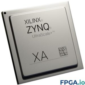
The XCZU28DR-2FFVG1517I is a Gen 1 Zynq UltraScale+ RFSoC from AMD (Xilinx), built on a 16 nm FinFET+ process. It is the SD-FEC-equipped member of the Gen 1 family: eight direct-RF-sampling ADCs, eight RF-DACs, eight hardened soft-decision forward error correction cores, a 64-bit quad-core Arm application processor and 930,300 UltraScale+ logic cells, all in a single 1517-ball flip-chip BGA. Because the converters sample directly at RF, a design built around the XCZU28DR-2FFVG1517I can delete the entire external IF chain — mixers, JESD204B links and discrete data converters — cutting board area, power and latency in one step.
This is the -2 speed grade, industrial temperature (I) ordering option, qualified from -40 °C to +100 °C junction temperature, which makes it the right choice for outdoor 5G radio units, vehicle and airborne platforms, and any enclosure that starts cold.
Key Technical Features
RF Data Converter Subsystem
- 8× RF-ADC — 12-bit resolution, up to 4.096 GSPS per channel, 2 channels per tile across 4 tiles. First Nyquist zone reaches ~2.048 GHz; bandpass undersampling extends usable input into higher Nyquist zones.
- 8× RF-DAC — 14-bit resolution, up to 6.554 GSPS per channel, with optional mix-mode operation to boost output power in the second Nyquist zone.
- Per-channel DDC / DUC — programmable decimation and interpolation (×1, ×2, ×4, ×8), 48-bit NCO per converter, full complex mixer, plus low-power fixed Fs/4 and Fs/2 modes.
- Single-band and multi-band operation from one tile, with 80% pass band and 89 dB stop-band attenuation on the decimation filters.
Hardened SD-FEC
Eight integrated soft-decision FEC blocks handle LDPC (including 5G NR and DOCSIS 3.1 configurations) and Turbo decode entirely in hard silicon. On the XCZU28DR-2FFVG1517I this frees the tens of thousands of LUTs a soft LDPC decoder would otherwise consume, and drops FEC power substantially versus a fabric implementation. This block is what separates the ZU28DR from the otherwise similar ZU27DR.
Processing System
- Quad-core Arm Cortex-A53 MPCore with NEON and single/double-precision FPU, 32 KB/32 KB L1 per core, 1 MB shared L2 — up to 1.333 GHz at -2 speed grade
- Dual-core Arm Cortex-R5F real-time processor with TCM, lock-step capable — up to 533 MHz
- 256 KB on-chip memory with ECC; external DDR4, DDR3, DDR3L, LPDDR4, LPDDR3, Quad-SPI, NAND and eMMC support
- 214 PS I/O with UART, CAN, USB 2.0, I2C, SPI, 32-bit GPIO, RTC, watchdog and triple timer counters
Programmable Logic
- 930,300 system logic cells · 425,280 CLB LUTs · 850,560 CLB flip-flops
- 4,272 DSP48E2 slices with 27×18 multipliers — the arithmetic budget for wideband digital front ends, beamforming and pulse compression
- 38.0 Mb block RAM (1,080 × 36 Kb, built-in FIFO and ECC) · 22.5 Mb UltraRAM (80 × 4K×72) · 13.0 Mb distributed RAM
- 299 HP I/O and 48 HD I/O in the FFVG1517 package
High-Speed Connectivity
- 16× GTY transceivers, up to 32.75 Gb/s at -2 speed grade — usable for PCIe Gen3/Gen4, 25G/100G Ethernet, CPRI and eCPRI fronthaul, and JESD204B/C to external converters
- 4× PS-GTR lanes up to 6.0 Gb/s for PCIe Gen2, SATA 3.1, USB 3.0, DisplayPort 1.2a and SGMII
- Integrated block for PCI Express (Gen3 ×16), 2× 100G Ethernet MAC/PCS with RS-FEC, 150G Interlaken
Security and Monitoring
Boot is handled by the Configuration Security Unit with 256-bit AES-GCM decryption and SHA/384 authentication; the same crypto engines are available to user applications after boot. The System Monitor tracks on-chip temperature and supply rails and can digitise up to 17 external analog inputs.
XCZU28DR-2FFVG1517I Specifications
| Manufacturer Part Number | XCZU28DR-2FFVG1517I |
| Manufacturer | AMD (Xilinx) |
| Family / Device | Zynq UltraScale+ RFSoC, Gen 1 — ZU28DR |
| Process | 16 nm FinFET+ |
| Speed Grade | -2 |
| Temperature Grade | Industrial (I), -40 °C to +100 °C Tj |
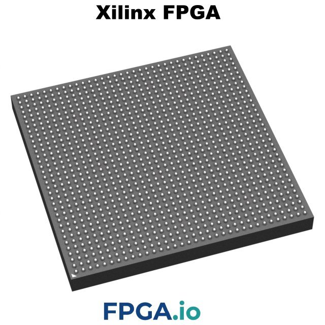
| Package | FFVG1517 — 1517-ball flip-chip BGA, 40 × 40 mm, 1.0 mm pitch |
| APU | Quad-core Arm Cortex-A53, up to 1.333 GHz |
| RPU | Dual-core Arm Cortex-R5F, up to 533 MHz |
| System Logic Cells | 930,300 |
| CLB LUTs / Flip-Flops | 425,280 / 850,560 |
| DSP Slices | 4,272 (DSP48E2) |
| Block RAM | 38.0 Mb (1,080 blocks) |
| UltraRAM | 22.5 Mb (80 blocks) |
| Distributed RAM | 13.0 Mb |
| RF-ADC | 8 channels, 12-bit, up to 4.096 GSPS |
| RF-DAC | 8 channels, 14-bit, up to 6.554 GSPS |
| SD-FEC | 8 hardened LDPC / Turbo cores |
| GTY Transceivers | 16, up to 32.75 Gb/s |
| PS-GTR Transceivers | 4, up to 6.0 Gb/s |
| PL I/O | 299 HP + 48 HD |
| PS I/O | 214 |
| Hard IP | PCIe Gen3 ×16, 2× 100G Ethernet w/ RS-FEC, 150G Interlaken |
| Design Tools | AMD Vivado Design Suite, Vitis, PetaLinux, RF Data Converter IP |
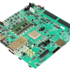
| Evaluation Kit | ZCU111 |
Part Number Decoded
- XC — Xilinx commercial device prefix
- ZU28DR — Zynq UltraScale+ RFSoC, 28DR density with SD-FEC
- -2 — speed grade 2 (the faster of the two grades offered on this device)
- FFVG1517 — lidded flip-chip BGA, 1517 balls, 40 × 40 mm, 1.0 mm pitch
- I — industrial temperature range, -40 °C to +100 °C junction
The related XCZU28DR-2FFVG1517E is the same die, package and speed grade with an extended (0 °C to +100 °C) rating. Choose the I suffix whenever ambient can fall below freezing. The FFVG1517 footprint is shared with the ZU25DR, ZU27DR, ZU43DR, ZU47DR and ZU48DR, so a board designed around the XCZU28DR-2FFVG1517I can migrate up or down in density without a PCB respin — verify power sequencing per DS926 before swapping.
Typical Applications
- 5G NR massive MIMO and remote radio units — direct RF sampling across sub-6 GHz bands with hardened LDPC in the same device
- Phased-array and multifunction radar — eight coherent transmit and receive chains with per-channel NCO for digital beamforming
- Electronic warfare and SIGINT — wideband spectrum capture with on-chip channelisation
- Cable infrastructure (DOCSIS 3.1) — full-band capture plus integrated soft-decision FEC
- Satellite ground terminals and SATCOM modems
- High-end test and measurement — signal generators, spectrum and vector analysers, ATE
- Software-defined radio platforms requiring CPRI/eCPRI or Ethernet-to-RF on one chip
Design Resources
Development uses the AMD Vivado Design Suite with the RF Data Converter IP core for tile configuration, plus Vitis and PetaLinux for the processing system. Reference documents: DS889 (RFSoC Overview), DS926 (DC and AC Switching Characteristics), UG1075 (packaging and pinouts — the FFVG1517 pin table ships as a spreadsheet), PG269 (RF Data Converter) and UG583 (PCB design and pin planning, including the ground-stitching guidance around the RF pins). The ZCU111 evaluation kit is the reference platform for this device.
Reviews
There are no reviews yet.