

Description
XCZU47DR-2FFVG1517I Overview
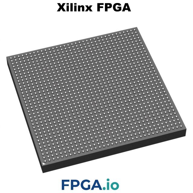
The XCZU47DR-2FFVG1517I is a third-generation AMD (formerly Xilinx) Zynq® UltraScale+™ RFSoC — a monolithic 16 nm FinFET+ device that integrates eight 14-bit RF-ADC channels, eight 14-bit RF-DAC channels, 930,300 system logic cells of UltraScale+ programmable logic, and a 64-bit quad-core Arm® Cortex®-A53 processing system in a single 1517-ball flip-chip BGA.
By sampling RF directly on-chip, the XCZU47DR-2FFVG1517I removes the external data converters and the JESD204B/C serial links that sit between them and the FPGA. The result is a substantial reduction in board area, power and signal-chain latency versus a discrete FPGA-plus-converter design — the reason this device appears in 5G radio units, phased-array radar, SATCOM terminals, wideband SDR and high-end test instrumentation.
Key Features of the XCZU47DR-2FFVG1517I
- Direct RF sampling — 8 × 14-bit RF-ADC at up to 5.0 GSPS and 8 × 14-bit RF-DAC at up to 9.85 GSPS, with RF input support to approximately 6 GHz.
- Integrated DDC/DUC — programmable decimation and interpolation, NCO and complex mixer per tile, with dual-band operation supported.
- Large DSP fabric — 4,272 DSP48E2 slices and 425,280 CLB LUTs for beamforming, DPD, channelisation and pulse compression.
- Heterogeneous processing — quad-core Cortex-A53 up to 1.33 GHz for Linux and control-plane software, plus dual-core Cortex-R5F up to 533 MHz for deterministic real-time loops.
- High-speed connectivity — 16 GTY transceivers (up to 28.21 Gb/s per lane at the −2 speed grade) and 4 PS-GTR lanes, with hardened PCIe® (Gen3 ×16 / Gen4 ×8), 100G Ethernet MAC/PCS with RS-FEC, and 150G Interlaken.
- Secure boot — Configuration Security Unit with AES-256-GCM, SHA-3/384 and RSA-4096.
- Industrial temperature grade — TJ −40 °C to +100 °C, suitable for outdoor radio, defence and rugged deployments.
XCZU47DR-2FFVG1517I Specifications
| Manufacturer | AMD (Xilinx) |
| Family / Generation | Zynq® UltraScale+™ RFSoC, Gen 3 |
| Process | 16 nm FinFET+ |
| Application Processor | Quad-core Arm Cortex-A53 MPCore with CoreSight, up to 1.33 GHz |
| Real-Time Processor | Dual-core Arm Cortex-R5F with CoreSight, up to 533 MHz |
| On-Chip Memory | 256 KB with ECC |
| System Logic Cells | 930,300 |
| CLB LUTs / Flip-Flops | 425,280 / 850,560 |
| DSP Slices (DSP48E2) | 4,272 |
| Block RAM | 38.0 Mb (1,080 blocks) |
| UltraRAM | 22.5 Mb (80 blocks) |
| Distributed RAM | 13.0 Mb |
| RF-ADC | 8 channels, 14-bit, up to 5.0 GSPS, with DDC |
| RF-DAC | 8 channels, 14-bit, up to 9.85 GSPS, with DUC |
| Max RF Input Frequency | Up to approx. 6 GHz |
| SD-FEC Blocks | None on ZU47DR (see XCZU48DR for 8 SD-FEC cores) |
| GTY Transceivers | 16, up to 28.21 Gb/s per lane (−2 speed grade) |
| PS-GTR Transceivers | 4 (USB 3.0, SATA 3.1, DisplayPort 1.2a, PCIe, SGMII) |
| Hardened IP | PCIe Gen3 ×16 / Gen4 ×8, 100G Ethernet with RS-FEC, 150G Interlaken |
| Memory Interfaces | DDR4 / DDR3 / DDR3L / LPDDR4 / LPDDR3 with ECC; Quad-SPI, NAND, eMMC/SD |
| Peripherals | Gigabit Ethernet, USB 2.0/3.0 OTG, CAN, I²C, SPI, UART, GPIO, DMA, WDT |
| Package | FFVG1517 — 1517-ball FCBGA, 40 × 40 mm, 1.0 mm pitch, lidded |
| Speed Grade | −2 |
| Temperature Grade | Industrial (I), TJ −40 °C to +100 °C |
| Core Voltage (VCCINT) | 0.9 V |
| Compliance | RoHS compliant, Pb-free (SAC305 balls) |
Specifications are for reference. Always verify against the current AMD DS889, DS926 and UG1075 revisions before design commit.
XCZU47DR-2FFVG1517I Part Number Breakdown
| XC | AMD Xilinx commercial silicon (XQ denotes defence grade) |
| ZU | Zynq UltraScale+ family |
| 47DR | Device 47, DR = RFSoC direct-RF variant |
| -2 | Speed grade 2 (higher performance than −1) |
| FF | Flip-chip, fine-pitch, lidded package |
| VG | Package ball-map identifier |
| 1517 | 1517 balls |
| I | Industrial temperature range, TJ −40 °C to +100 °C |
Applications
- 5G NR sub-6 GHz radio units and 8T8R massive MIMO front-haul
- Phased-array and digital-array radar, electronic warfare and SIGINT receivers
- Satellite communications and ground-station modems
- Wideband software-defined radio and cognitive radio
- DOCSIS 3.1 / 4.0 Remote PHY nodes for cable distributed access
- Signal generators, spectrum analysers and high-channel-count test equipment
- LiDAR and instrumentation-grade data acquisition
XCZU47DR vs XCZU48DR vs XCZU28DR
| Device | Gen | RF-ADC | RF-DAC | SD-FEC | Logic Cells |
| XCZU28DR | Gen 1 | 8 × 12-bit, 4.096 GSPS | 8 × 14-bit, 6.554 GSPS | 8 | 930,300 |
| XCZU47DR | Gen 3 | 8 × 14-bit, 5.0 GSPS | 8 × 14-bit, 9.85 GSPS | None | 930,300 |
| XCZU48DR | Gen 3 | 8 × 14-bit, 5.0 GSPS | 8 × 14-bit, 9.85 GSPS | 8 | 930,300 |
In short: choose the XCZU47DR-2FFVG1517I when you need Gen 3 converter performance and wide DSP fabric but handle forward error correction elsewhere. If your system needs hardened LDPC or Turbo FEC for 5G NR, LTE or DOCSIS, specify the XCZU48DR instead.
Footprint-Compatible Alternatives
The FFVG1517 and FSVG1517 ball maps are shared across several RFSoC densities, so a board designed for the XCZU47DR-2FFVG1517I can generally accept XCZU25DR, XCZU27DR, XCZU28DR, XCZU43DR and XCZU48DR devices without a PCB respin. Confirm power-sequencing differences in AMD DS926 before substituting. The FSVG1517 variant is the lidless equivalent with the same ball map, chosen where package height matters.
Design Resources
Develop with AMD Vivado® Design Suite and the Vitis™ unified software platform, using the RF Data Converter IP to configure ADC/DAC tiles, mixers and NCOs. PYNQ supports Python-based rapid prototyping on the Cortex-A53. Reference documentation: DS889 (overview), DS926 (DC and AC switching characteristics), UG583 (PCB design) and UG1075 (packaging and pinouts).
Ordering, Quality and Shipping
- Genuine AMD Xilinx product, factory-sealed in original tray packaging
- ESD and moisture-sensitivity handling per JEDEC J-STD-033
- Full traceability with date and lot code on request
- Volume pricing, lead-time quotations and BOM sourcing available
- Worldwide shipping with export documentation support
Need pricing, stock or a matched quantity of the XCZU47DR-2FFVG1517I? Contact our team for a same-day quotation.
Frequently Asked Questions
What is the difference between XCZU47DR-2FFVG1517I and XCZU47DR-2FSVG1517I?
Both share the same ball map and electrical specification. FFVG1517 is lidded; FSVG1517 is lidless with a stiffener ring, giving a lower package height for module and SoM designs but requiring more careful handling during assembly and rework.
Does the XCZU47DR-2FFVG1517I include SD-FEC?
No. The XCZU47DR has no soft-decision FEC cores. The pin-compatible XCZU48DR provides eight SD-FEC blocks supporting LDPC encode/decode and Turbo decode.
What does the “-2” and “I” mean in XCZU47DR-2FFVG1517I?
“-2” is the speed grade, giving higher fabric, processor and transceiver performance than the −1 grade. “I” is the industrial temperature grade, rated from −40 °C to +100 °C junction temperature.
Does it support PCIe Gen4?
Yes. The integrated PCIe block supports Gen3 at up to ×16 or Gen4 at up to ×8 (16 GT/s).
What RF input frequency does it handle?
RF-ADC inputs are specified to approximately 6 GHz with an appropriate balun. At 5 GSPS the first Nyquist zone is 2.5 GHz; higher Nyquist zones can be used for sub-sampling up to the maximum input frequency.
Reviews
There are no reviews yet.