
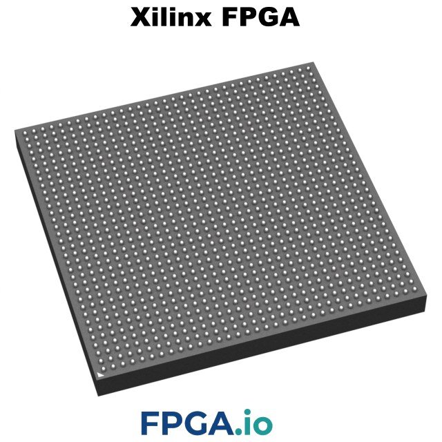

Description
XCZU48DR-2FFVG1517I Overview
The XCZU48DR-2FFVG1517I is a Gen 3 member of the AMD (formerly Xilinx) Zynq UltraScale+ RFSoC family, built on a 16 nm FinFET+ process. It combines a direct-RF sampling data converter subsystem, hardened Soft-Decision Forward Error Correction, a 64-bit Arm application processor complex and a large UltraScale+ programmable logic fabric in a single 1517-ball FCBGA. The result is a monolithic radio platform that removes the external data converters, JESD204B/C interfaces and companion FEC ASICs normally required in a multi-channel wideband radio card.
Within the Gen 3 line-up, the XCZU48DR is the SD-FEC-enabled device. Its closest sibling, the XCZU47DR, shares the same programmable logic and converter counts but contains no SD-FEC blocks. If your design terminates 5G NR, DOCSIS 3.1 or Wi-Fi channel coding on-chip, the XCZU48DR-2FFVG1517I is the correct part number.
RF Data Converter Subsystem (Gen 3)
The Gen 3 converter subsystem is arranged as four RF-ADC tiles and four RF-DAC tiles, each carrying two converters.
- 8 × RF-ADC — 14-bit resolution, up to 5.0 GSPS, analog input frequency up to 6 GHz, enabling direct sampling in the second and third Nyquist zones.
- 8 × RF-DAC — 14-bit resolution, up to 9.85 GSPS, with inverse-sinc compensation and Gen 3 digital mixer modes for high-Nyquist synthesis.
- Integrated DDC / DUC — per-converter digital down- and up-conversion with 48-bit NCOs and programmable decimation and interpolation factors, moving channelisation out of the fabric and cutting DSP and power budgets.
- On-chip PLLs and multi-tile synchronisation for deterministic, repeatable phase alignment across all converters — essential for phased-array beamforming and MIMO.
Because the converters sit on-die, the JESD204B/C SerDes links, retimers and clock trees of a discrete converter design disappear, along with their board area, insertion loss and latency.
Soft-Decision FEC — the XCZU48DR Differentiator
The XCZU48DR-2FFVG1517I integrates eight hardened SD-FEC cores. Each core supports:
- LDPC encode and decode with fully user-programmable parity-check matrices, covering 5G NR, DOCSIS 3.1 and IEEE 802.11 code sets;
- Turbo decode for LTE and legacy 3GPP air interfaces;
- Run-time code switching, so a single bitstream can service multiple numerologies or standards.
Implementing the same throughput in soft logic would consume a large fraction of the fabric and a disproportionate share of the power budget. The hardened blocks free that capacity for beamforming, DPD, DFE and application logic.
Programmable Logic Resources
| System Logic Cells | 930,300 |
| CLB LUTs | 425,280 |
| CLB Flip-Flops | 850,560 |
| DSP Slices (DSP48E2) | 4,272 |
| Block RAM | 38.0 Mb (1,080 blocks of 36 Kb) |
| UltraRAM | 22.5 Mb (80 blocks of 288 Kb) |
| Total On-Chip RAM | 60.5 Mb |
Processing System (PS)
- Application Processing Unit: quad-core Arm Cortex-A53, up to 1.33 GHz at the −2 speed grade, with NEON and single/double-precision FPU.
- Real-Time Processing Unit: dual-core Arm Cortex-R5F at 533 MHz, with lock-step operation and TCM for deterministic control tasks.
- On-Chip Memory: 256 KB OCM with ECC.
- Memory Controller: 72-bit (64 + 8 ECC) PS DDR4 / LPDDR4 interface; the PL supports independent DDR4 controllers.
- Peripherals: Gigabit Ethernet, USB 3.0, SD/eMMC, SPI, QSPI, I2C, CAN, UART, GPIO.
- Security: AES-GCM bitstream decryption, RSA authentication, SHA-3/384, secure boot and configuration security unit.
Note on GPU: Zynq UltraScale+ RFSoC devices, including the XCZU48DR, do
Reviews
There are no reviews yet.