
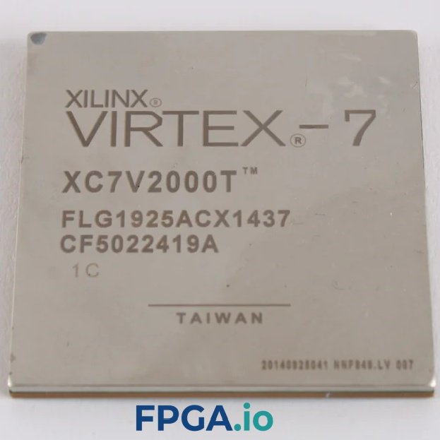

Description
The XCVU13P-2FHGB2104I is an AMD (Xilinx) Virtex UltraScale+ FPGA delivering 3.78 million logic cells, 12,288 DSP48E2 slices, and 454.5 Mb of on-chip memory in a 2104-ball FCBGA package. Speed grade -2, industrial temperature range (-40 °C to +100 °C). Ideal for data-center acceleration, 100G+ networking, machine-learning inference, aerospace/defense signal processing, and high-performance computing. RoHS 3 compliant. In stock at FPGA.io.
XCVU13P-2FHGB2104I — AMD Xilinx Virtex UltraScale+ FPGA
The XCVU13P-2FHGB2104I is one of the highest-capacity members of AMD’s Virtex® UltraScale+™ FPGA family. Built on TSMC’s 16 nm FinFET+ process and leveraging third-generation stacked silicon interconnect (SSI) technology, it packs 3.78 million logic cells, 12,288 DSP slices, and over 454 Mb of on-chip memory into a single 2104-pin flip-chip BGA package—all while operating across the full industrial temperature range of −40 °C to +100 °C.
Whether you are designing next-generation 100G/400G network infrastructure, deploying real-time AI inference at the edge, or building safety-critical aerospace and defense platforms, the XCVU13P-2FHGB2104I provides the logic density, memory bandwidth, and serial I/O capacity to consolidate workloads that would otherwise require multiple devices.
Part Number Breakdown: XCVU13P-2FHGB2104I
| Segment | Meaning |
|---|---|
| XCVU13P | Virtex UltraScale+ VU13P die |
| -2 | Speed grade -2 (standard performance) |
| F | Flip-chip package technology |
| HGB | Package variant / ball-map code |
| 2104 | 2,104-ball FCBGA (47.5 mm × 47.5 mm) |
| I | Industrial temp range: −40 °C to +100 °C (TJ) |
XCVU13P-2FHGB2104I Key Specifications
| Parameter | Value |
|---|---|
| Manufacturer | AMD (formerly Xilinx) |
| Family / Series | Virtex® UltraScale+™ |
| Process Node | 16 nm FinFET+ (TSMC) |
| System Logic Cells | 3,780,000 |
| CLB LUTs (6-input) | 1,728,000 |
| CLBs / LABs | 216,000 |
| Max. Distributed RAM | 48.3 Mb |
| Block RAM (36 Kb each) | 2,688 blocks — 94.5 Mb |
| UltraRAM (288 Kb each) | 1,280 blocks — 360 Mb |
| Total On-Chip Memory | ~514.9 Mb (Distributed + Block RAM + UltraRAM) |
| DSP Slices (DSP48E2) | 12,288 |
| DSP Performance | Up to 38 TOPs INT8 / 22 TeraMACs |
| Max. User I/O (HP) | 702 |
| GTY Transceivers | Up to 128 (32.75 Gb/s line rate each) |
| PCIe® Hard Block | Gen3 ×16 |
| 100G Ethernet MAC | Integrated |
| 150G Interlaken | Integrated |
| DDR4 Interface Speed | Up to 2,666 Mb/s |
| Clock Management | MMCM, PLL |
| Max. Operating Frequency | 775 MHz |
| Core Supply Voltage (VCCINT) | 0.825 V – 0.876 V |
| I/O Supply Voltage | Up to 3.3 V |
| Operating Temperature | −40 °C to +100 °C (TJ) — Industrial |
| Package | 2104-ball FCBGA (47.5 × 47.5 mm) |
| SSI Technology | Yes — 3rd-gen stacked silicon interconnect |
| RoHS Status | RoHS 3 Compliant |
| Product Status | Active / Production |
Virtex UltraScale+ Architecture Highlights
3D-on-3D Stacked Silicon Interconnect (SSI)
The XCVU13P uses AMD’s third-generation SSI technology to combine multiple super logic regions (SLRs) on a single silicon interposer. Registered inter-die routing lines operate above 600 MHz, delivering a virtual monolithic experience without the yield or reticle-size limitations of a single-die approach. For the system designer this means more usable logic, wider internal buses, and fewer board-level device-to-device links.
DSP48E2 Compute Engine
Each of the 12,288 DSP48E2 slices integrates a 27 × 18 multiplier, 48-bit accumulator, 96-bit XOR, and a 27-bit pre-adder in a single hardened block. In INT8 mode the array delivers up to 38 trillion operations per second—enough for real-time neural-network inference on large models without a discrete GPU. Fixed-point and single-precision floating-point MAC operations run in a single clock cycle.
On-Chip Memory Hierarchy
The device’s three-tier memory architecture—distributed LUT RAM, 36 Kb Block RAM with built-in FIFO and ECC, and 288 Kb UltraRAM—totals over 500 Mb of on-chip storage. UltraRAM blocks cascade to form deep, wide memory structures ideal for packet buffering, video line stores, and coefficient caches, all without consuming general-purpose routing. A deep-sleep mode lets UltraRAM retain data while cutting static power.
High-Speed Serial I/O
Up to 128 GTY transceivers operate at line rates to 32.75 Gb/s, supporting backplane, chip-to-optics, and chip-to-chip links. Hardened 100G Ethernet MAC, 150G Interlaken, and PCIe Gen3 ×16 IP blocks eliminate the need for soft-core implementations, saving LUT resources and simplifying timing closure.
Target Applications for the XCVU13P-2FHGB2104I
- Data-Center & Cloud Acceleration — SmartNIC offload, storage compression/decompression, database query acceleration, and in-line encryption.
- 100G / 400G Networking — High-port-density switches, routers, firewalls, and DPI engines leveraging hardened Ethernet and Interlaken cores.
- AI & Machine-Learning Inference — INT8 and fixed-point inference pipelines running at up to 38 TOPs with deterministic, low-latency response.
- Aerospace & Defense — Radar/EW signal processing, SIGINT, software-defined radio (SDR), and AESA beamforming with industrial-grade temperature tolerance.
- High-Performance Computing (HPC) — Financial-market tick-to-trade, genomics sequencing pipelines, and Monte Carlo simulation acceleration.
- Broadcast & Pro Video — Real-time 8K encoding/decoding, multi-channel video switching, and frame-buffer management using on-chip UltraRAM.
- Test & Measurement — High-speed data acquisition, arbitrary waveform generation, and protocol analysis for next-generation interfaces.
- Wired & Wireless Infrastructure — 5G fronthaul/backhaul, OTN muxponders, and coherent optical DSP.
Why Buy XCVU13P-2FHGB2104I from FPGA.io?
- Authentic AMD (Xilinx) Stock — Every XCVU13P-2FHGB2104I unit is sourced through authorized channels and fully traceable.
- Competitive Pricing — Volume discounts available. Request a quote for project-quantity pricing.
- Global Shipping — Fast, insured worldwide delivery with full export-compliance documentation.
- Technical Support — Our FPGA engineers can assist with package selection, thermal design guidance, and migration from earlier Virtex generations.
Related Virtex UltraScale+ Part Numbers
| Part Number | Logic Cells | DSP Slices | Notes |
|---|---|---|---|
| XCVU9P-2FLGA2104I | 2,586,000 | 6,840 | Lower density, same footprint family |
| XCVU11P-2FLGA2104I | 2,592,000 | 9,216 | Mid-range density, pin-compatible options |
| XCVU13P-2FHGA2104I | 3,780,000 | 12,288 | Alternate package variant of the same die |
| XCVU13P-3FHGB2104I | 3,780,000 | 12,288 | Higher speed grade (-3) version |
Frequently Asked Questions
What is the XCVU13P-2FHGB2104I?
The XCVU13P-2FHGB2104I is a high-density FPGA (Field Programmable Gate Array) from AMD’s Virtex UltraScale+ family. It contains 3.78 million logic cells, 12,288 DSP slices, and over 454 Mb of on-chip memory in a 2104-pin FCBGA package, with an industrial operating temperature range of −40 °C to +100 °C.
What speed grade is the XCVU13P-2FHGB2104I?
The “-2” suffix indicates speed grade -2, which is the standard performance tier in the Virtex UltraScale+ lineup. A “-3” variant is available for applications that require faster timing at higher power.
Is the XCVU13P-2FHGB2104I RoHS compliant?
Yes. This part is RoHS 3 (EU Directive 2015/863) compliant and carries a lead-free (Pb-free) ball finish.
What is the operating temperature range?
The “I” suffix designates the industrial temperature grade: junction temperature (TJ) from −40 °C to +100 °C.
What design tools support the XCVU13P?
AMD Vivado™ Design Suite (Vivado ML Edition for AI-optimized flows) fully supports synthesis, implementation, timing analysis, and debug for all Virtex UltraScale+ devices including the XCVU13P.
Can the XCVU13P-2FHGB2104I be used for AI inference?
Yes. With 12,288 DSP48E2 slices running INT8 multiply-accumulate operations, the device delivers up to 38 TOPs of inference throughput, making it a strong alternative to dedicated accelerators when design flexibility and low, deterministic latency are priorities.
What package does the XCVU13P-2FHGB2104I use?
It ships in a 2104-ball flip-chip BGA (FCBGA) package measuring 47.5 mm × 47.5 mm with a 1.0 mm ball pitch.
Reviews
There are no reviews yet.