
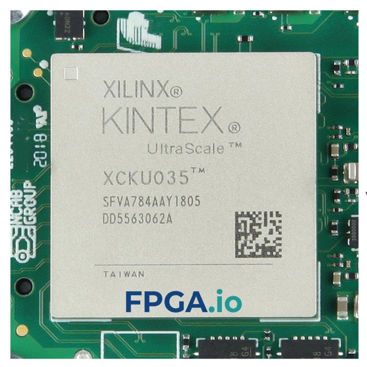

Description
Kintex-7 price/performance in a compact 23 × 23 mm package
The XC7K70T-1FBG484I is the entry point into AMD’s (formerly Xilinx) Kintex-7 family — the 28 nm HKMG series positioned for the best price/performance/watt in the 7 Series. It packs 65,600 logic cells, 240 DSP48E1 slices and 4,860 Kb of block RAM into a 484-ball lidless flip-chip BGA measuring just 23 × 23 mm, making it a strong fit for designs that need serious signal-processing throughput on a board where space and power budget are both tight.
Unlike lower-cost families, this device brings both HP and HR I/O banks to the same package: 100 high-performance pins for 1.2 V–1.8 V memory and high-speed interfaces, plus 185 high-range pins covering 1.2 V–3.3 V for legacy peripherals and level-flexible control signals. That combination lets a single device drive a DDR3 interface at up to 1,866 Mb/s while still talking directly to 3.3 V sensors, ADCs and microcontrollers — usually without external level translation.
Serial connectivity and hard IP
Four GTX multi-gigabit transceivers are bonded out in the FBG484 package, rated to 10.3 Gb/s. One integrated block for PCI Express is included, configurable as Endpoint or Root Port up to x8 Gen2. Six clock management tiles (each an MMCM plus a PLL) handle frequency synthesis, phase shifting and jitter filtering, and the on-die XADC provides dual 12-bit 1 MSPS converters with on-chip temperature and supply-rail monitoring — useful for closed-loop thermal management without adding external parts.
Industrial grade, production ready
The “I” suffix specifies an industrial junction temperature range of –40 °C to +100 °C at a 1.0 V core, suited to uncontrolled enclosures, outdoor cabinets and factory-floor equipment. Configuration options include SPI (x1/x2/x4) and BPI parallel-NOR flash, JTAG and slave modes, with 256-bit AES bitstream encryption plus HMAC/SHA-256 authentication, MultiBoot with safe update, built-in SEU detection and correction, and support for partial reconfiguration.
Easy migration path
The XC7K160T is footprint-compatible in the same FBG484 package with identical I/O and transceiver counts, so a board designed around this device can be re-spun to roughly 2.5× the logic capacity without touching the PCB layout.
Specifications
| Manufacturer | AMD (Xilinx) |
| Manufacturer Part Number | XC7K70T-1FBG484I |
| Family | Kintex-7, 28 nm HKMG HPL |
| Logic Cells | 65,600 |
| Slices | 10,250 |
| Max Distributed RAM | 838 Kb |
| Block RAM | 4,860 Kb (135 × 36 Kb blocks) |
| DSP Slices (DSP48E1) | 240 |
| Clock Management Tiles | 6 (MMCM + PLL each) |
| PCI Express | 1 integrated block, up to x8 Gen2 |
| Transceivers | 4 × GTX in FBG484, up to 10.3 Gb/s |
| Analog | 1 × XADC, dual 12-bit 1 MSPS |
| Max User I/O | 285 (185 HR + 100 HP) |
| I/O Banks | 6 (excluding config bank 0) |
| I/O Voltage | 1.2–3.3 V (HR) / 1.2–1.8 V (HP) |
| Memory Interface | DDR3 up to 1,866 Mb/s |
| Core Voltage | 1.0 V |
| Speed Grade | -1 |
| Temperature Grade | Industrial, Tj –40 °C to +100 °C |
| Package | FBG484, 484-ball lidless flip-chip BGA |
| Body Size / Ball Pitch | 23 × 23 mm / 1.0 mm |
| Mounting | Surface mount (SMD/SMT) |
| RoHS | Pb-free, RoHS compliant |
| Design Tools | AMD Vivado Design Suite |
Typical Applications
Wireless infrastructure and remote radio heads · software-defined radio · machine vision and industrial cameras · medical imaging front-ends (ultrasound, CT) · test and measurement instruments · high-speed data acquisition · PCIe add-in cards · broadcast and video processing · industrial networking and motor control · aerospace and defense subsystems
Reviews
There are no reviews yet.