

Description
AMD Xilinx XCZU47DR-2FFVE1156I – Zynq UltraScale+ RFSoC Gen3 System-on-Chip
The XCZU47DR-2FFVE1156I is a Gen3 member of AMD’s (formerly Xilinx) Zynq UltraScale+ RFSoC family. It monolithically integrates direct-RF-sampling data converters, a heterogeneous Arm processing system, and UltraScale+ programmable logic on one 16 nm FinFET+ die. That integration eliminates the external JESD204 link, the discrete ADC/DAC clock tree, and the separate host SoC that a conventional radio front end would need, cutting board area, power, and latency in software-defined radio designs.
RF Data Converters (Gen3)
- 8 × RF-ADCs, 14-bit, sample rate up to 5.0 GSPS, with integrated digital down-converters (DDCs), programmable decimation, NCO, and complex mixer
- 8 × RF-DACs, 14-bit, sample rate up to 9.85 GSPS, with integrated digital up-converters (DUCs) and programmable interpolation
- Dual-band operation supported on DDC/DUC signal paths
- Best-in-class noise spectral density for wideband multi-carrier signals
Soft-Decision Forward Error Correction (SD-FEC)
- Hardened LDPC encoder/decoder for 5G NR and DOCSIS 3.1
- Hardened Turbo decoder for LTE
- Offloads high-throughput channel coding from the fabric and PS
Processing System (PS)
- Quad-core Arm Cortex-A53 application processor, up to 1.333 GHz, running Linux
- Dual-core Arm Cortex-R5F real-time processor, up to 533 MHz
- Arm Mali-400 MP2 GPU
- 256 KB on-chip RAM, DDR4 memory controller
- Full peripheral set: Gigabit Ethernet, USB 3.0/2.0, SATA 3.1, PCIe Gen2/Gen3, DisplayPort, SD/eMMC, QSPI, UART, I²C, SPI, CAN
Programmable Logic (PL)
- ~930,000 UltraScale+ system logic cells
- ~4,272 DSP48E2 slices
- Distributed Block RAM and UltraRAM
- Multi-gigabit GTY transceivers for high-speed serial links
Security & System Monitoring
- Configuration Security Unit (CSU) with 256-bit AES-GCM and SHA-384 secure boot
- Cryptographic engines available to user application after boot
- On-die System Monitor for voltage and temperature telemetry
Package & Ordering Information
| Attribute | Value |
|---|---|
| Manufacturer | AMD (Xilinx) |
| Part Number | XCZU47DR-2FFVE1156I |
| Family | Zynq UltraScale+ RFSoC, Gen3 |
| Process | 16 nm FinFET+ |
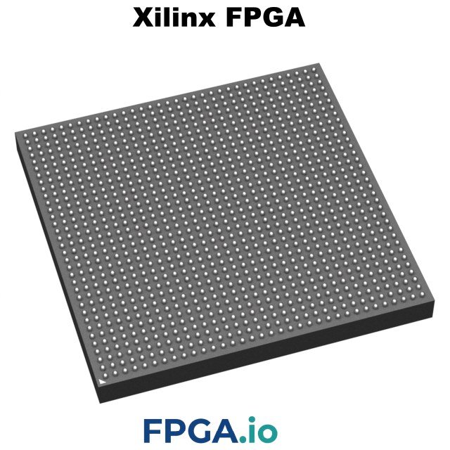
| Package | FFVE1156, 35 × 35 mm, 1156-ball flip-chip BGA |
| Speed Grade | -2 |
| Temperature Grade | Industrial, -40 °C to +100 °C (TJ) |
| RoHS | Compliant |
| Lifecycle | Active Production |
Target Applications
- 5G NR baseband and massive MIMO radio units
- Fixed wireless access (FWA) and small-cell backhaul
- Phased-array radar and digital array radar
- Electronic warfare, SIGINT, and spectrum monitoring
- Software-defined radio (SDR) platforms
- DOCSIS 3.1 cable TV access
- Satellite communication payloads and ground gateways
- High-channel-count test and measurement instrumentation
Design Enablement
Because the XCZU47DR integrates the RF signal chain on-die, PCB layout, power delivery network, and thermal design deserve more attention than in a discrete FPGA + converter architecture. Recommended tool flow includes the AMD Vivado Design Suite, PYNQ, MATLAB/Simulink with RFSoC support, and the AMD RF Data Converter IP. Reference platforms include the ZCU216 evaluation kit and third-party RFSoC Gen3 SoMs.
Availability at FPGA.io
FPGA.io stocks the XCZU47DR-2FFVE1156I in original factory packaging with full traceability. Bulk tray, cut tape, and moisture-controlled bagging available. Contact us for volume pricing, lead-time quotes, and datasheet access.
Reviews
There are no reviews yet.