
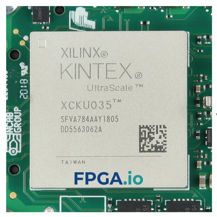

Description
XCKU15P-2FFVE1517I Overview
The XCKU15P-2FFVE1517I is a high-density FPGA from the AMD Xilinx
Kintex UltraScale+ family, fabricated on a 16 nm FinFET+ process. It pairs
1,143,450 system logic cells with on-chip UltraRAM and hardened connectivity IP,
making it a cost-effective alternative to Virtex-class devices for Nx100G
networking, wireless MIMO, packet processing and DSP-heavy designs.
This ordering code specifies the -2 speed grade in the
FFVE1517 package with the I (industrial)
temperature grade, rated from -40 °C to +100 °C junction temperature.
XCKU15P-2FFVE1517I Specifications
| Manufacturer | AMD (Xilinx) |
|---|---|
| Manufacturer Part Number | XCKU15P-2FFVE1517I |
| Family / Device | Kintex UltraScale+ / XCKU15P |
| Process Technology | 16 nm FinFET+ |
| System Logic Cells | 1,143,450 |
| CLB LUTs | 522,720 |
| CLB Flip-Flops | 1,045,440 |
| Max. Distributed RAM | 9.8 Mb |
| Total Block RAM | 34.6 Mb |
| UltraRAM | 36.0 Mb |
| DSP Slices (DSP48E2) | 1,968 |
| Clock Management Tiles | 11 |
| Integrated PCIe Gen3 x16 | 5 blocks |
| 100G Ethernet MAC w/ RS-FEC | 4 blocks |
| 150G Interlaken | 4 blocks |
| GTH Transceivers | 32 channels @ 16.3 Gb/s |
| GTY Transceivers | 24 channels @ 32.75 Gb/s |
| User I/O (this package) | 512 (96 HD + 416 HP) |
| Speed Grade | -2 |
| Temperature Grade | I — Industrial, -40 °C to +100 °C (Tj) |
| VCCINT (nominal) | 0.85 V |
| Package | FFVE1517 — 1517-ball FCBGA |
| Package Size / Ball Pitch | 40 × 40 mm / 1.0 mm |
| RoHS / Pb-Free | Yes |
| Design Software | AMD Vivado Design Suite |
Decoding the XCKU15P-2FFVE1517I Part Number
- XC — Xilinx commercial-grade programmable device
- KU15P — Kintex UltraScale+, 15P logic density
- -2 — speed grade (-1 slowest, -3 fastest; -3 is extended temp only)
- FFV — flip-chip BGA, Pb-free / RoHS-compliant
- E1517 — E footprint identifier, 1517 balls
- I — industrial temperature grade, -40 °C to +100 °C
Transceivers, PCIe and Hardened Connectivity
The FFVE1517 package exposes 56 serial transceiver channels on the XCKU15P:
32 GTH channels running to 16.3 Gb/s and 24 GTY channels running to 32.75 Gb/s.
Five integrated PCI Express Gen3 x16 blocks, four hardened 100G Ethernet MACs
with RS-FEC, and four 150G Interlaken cores remove the need to burn fabric on
soft protocol IP — AMD estimates the integrated Interlaken block alone saves
roughly 300K LUTs.
Typical Applications
- 5G radio units, remote radio heads and wireless MIMO baseband
- Nx100G line cards, switches and packet processing
- SmartNICs and data-centre acceleration
- DSP-intensive radar, SDR and signal-intelligence platforms
- Aerospace, defence and industrial imaging systems
- Test, measurement and high-speed data acquisition
Design Resources
Design entry, synthesis and implementation for the XCKU15P-2FFVE1517I are
handled in the AMD Vivado Design Suite. Key reference documents are the
Kintex UltraScale+ FPGAs Data Sheet (DS922), UltraScale Architecture and Product
Overview (DS890), UltraScale and UltraScale+ Packaging and Pinouts (UG575) and
the UltraScale Architecture PCB Design User Guide (UG583).
Ordering the XCKU15P-2FFVE1517I
All devices are supplied new, original and in factory packaging with full
traceability. Trays are standard; smaller quantities can be supplied in
anti-static packaging. Contact us for current stock, date codes, volume pricing
and lead time on the XCKU15P-2FFVE1517I and other Kintex UltraScale+ devices.
Frequently Asked Questions
What is the difference between XCKU15P-2FFVE1517I and XCKU15P-2FFVE1517E?
Only the temperature grade. The I suffix is industrial
(-40 °C to +100 °C junction), while E is extended
(0 °C to +100 °C junction). Logic resources, package and speed grade are identical.
How many transceivers does the XCKU15P-2FFVE1517I have?
56 in total for this package: 32 GTH channels at up to 16.3 Gb/s and 24 GTY
channels at up to 32.75 Gb/s.
Is it footprint compatible with the XCKU11P in the same package?
Yes — the XCKU11P-2FFVE1517I shares the E1517 footprint identifier, so the two
are footprint compatible. The XCKU11P offers 20 GTY channels versus 24 on the
XCKU15P, so confirm your transceiver and bank usage against UG575 and UG583
before committing to a migration path.
Is the XCKU15P-2FFVE1517I RoHS compliant?
Yes. The V in the FFVE package code denotes a Pb-free,
RoHS-compliant package.
Which software do I need?
AMD Vivado Design Suite. The XCKU15P is supported by the licensed Vivado
editions rather than the free WebPACK tier.
Reviews
There are no reviews yet.