Why PCB Manufacturing Cost Matters More Than Ever for FPGA Projects
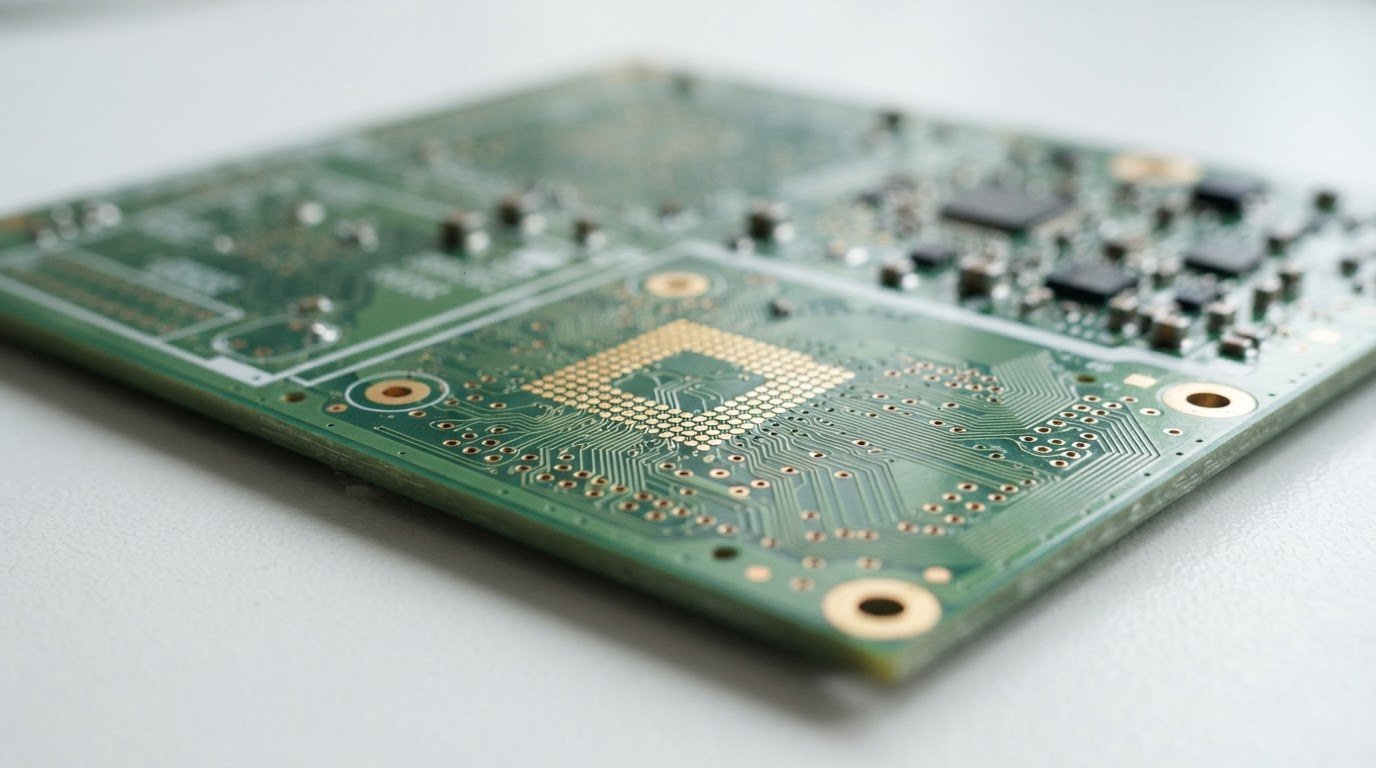
PCB manufacturing cost is one of the most significant—and most misunderstood—budget items in any FPGA development program. Modern FPGAs, whether you’re working with a small Lattice iCE40 or a massive Xilinx Versal, place extreme demands on the printed circuit board underneath them. BGA packages with 1,500+ pins, multi-gigabit SerDes lanes requiring precise impedance control, and power delivery networks that must supply hundreds of amps collectively push PCB complexity upward. That complexity translates directly into higher fabrication expenses.
Understanding where your money goes lets you make smarter trade-offs during schematic capture and layout, long before Gerber files reach the fab house. In this guide we dissect every major cost driver, provide realistic 2026 price ranges, and share practical strategies FPGA designers use to keep budgets under control.
The 10 Biggest Drivers of PCB Manufacturing Cost
1. Layer Count
Layer count is the single largest lever on PCB manufacturing cost. Each additional copper layer adds lamination cycles, drilling passes, and imaging steps. A rule of thumb for 2026 pricing:
| Layer Count | Relative Cost (vs. 2-layer) | Typical FPGA Use Case |
|---|---|---|
| 2 layers | 1× | Simple CPLD breakout boards |
| 4 layers | 1.8–2.2× | Low-pin-count FPGAs, evaluation boards |
| 6–8 layers | 3–4.5× | Mid-range FPGAs (Artix, ECP5) |
| 10–16 layers | 5–9× | High-speed FPGAs (Kintex, Agilex) |
| 18–24+ layers | 10–20× | Large Virtex / Versal / Stratix designs |
Before defaulting to more layers, audit your design. Sometimes rearranging the pin assignment inside the FPGA or switching to a different package variant eliminates two layers—and a significant chunk of cost. For detailed guidance on high-layer-count boards, see our resource on FPGA PCB fabrication with HDI and controlled impedance.
2. Board Material (Substrate)
Standard FR-4 (Tg 140 °C) is the cheapest option. High-speed FPGA designs often require mid-loss or low-loss laminates such as Megtron 6, Isola I-Speed, or Rogers materials for multi-gigabit lanes. Expect these specialty laminates to add 30–100 % to the base material cost. Hybrid stackups—Rogers on outer layers, standard FR-4 in the core—offer a middle ground.
3. HDI Features (Microvias, Blind/Buried Vias)
Fine-pitch BGA FPGAs (0.8 mm or 0.65 mm pitch) almost always need HDI technology. Each HDI “build-up” adds a sequential lamination cycle. Key cost impacts:
- 1+N+1 HDI: Adds ~25–40 % over a conventional through-hole board of the same layer count.
- 2+N+2 HDI: Adds ~50–80 %.
- Any-layer HDI (ELIC): Adds 100 %+ but enables the densest FPGA fan-outs.
4. Board Size and Panelization
Fab houses charge per panel, not per board. Smaller boards that nest efficiently into a standard 18 × 24″ panel yield more pieces per run and lower per-unit cost. Always ask your fabricator about optimal panel utilization before finalizing the board outline.
5. Minimum Trace Width and Spacing
Standard 5/5 mil (125/125 µm) trace/space is the sweet spot for cost. Dropping to 4/4 mil moves you into the “fine line” tier, and 3/3 mil requires advanced imaging equipment—each step roughly doubles the imaging cost component. FPGA BGA fan-out often dictates these minimums, so choosing a larger-pitch package when possible directly reduces your overall PCB manufacturing cost.
6. Drill Hole Sizes and Aspect Ratios
Mechanical drilling is cheap down to about 0.2 mm. Below that, laser drilling is required. Boards with aspect ratios above 10:1 (hole depth ÷ diameter) need specialized processes. A 16-layer board at 2.4 mm thickness with 0.2 mm vias is right at the limit—push past it and costs jump.
7. Surface Finish
The surface finish protects exposed copper and affects solderability. Cost ranking from low to high:
- HASL (leaded): Cheapest, but not flat enough for fine-pitch BGA.
- Lead-free HASL: Slightly more expensive, same flatness issue.
- ENIG: The default for FPGA boards—excellent flatness, ~15–25 % premium.
- ENEPIG: Needed for mixed assembly (gold wire bonding + soldering), ~30–40 % premium.
- Hard gold: Edge connectors only; expensive per area.
8. Impedance Control and Testing
Virtually every FPGA board requires controlled impedance on differential pairs (LVDS, HDMI, PCIe, DDR). The fabricator must run TDR coupon tests per panel. This adds $50–$150 per unique impedance class to NRE, plus ongoing per-panel testing costs. Consolidating impedance targets (e.g., standardizing on 50 Ω single-ended / 100 Ω differential) reduces test overhead.
9. Solder Mask and Silkscreen
Standard green LPI solder mask is included in base pricing. Matte black, white, or other colors carry a small surcharge ($20–$50 per batch in prototype quantities). More impactful is solder-mask-defined (SMD) vs. non-solder-mask-defined (NSMD) pad design for BGA—this affects yield, not direct fab cost, but rework costs can dwarf the original PCB price.
10. Volume and Lead Time
This is where PCB manufacturing cost varies the most dramatically:
| Quantity | Typical Price Per Board (8-layer, 100×100 mm) | Lead Time |
|---|---|---|
| 1–5 pcs (prototype) | $80–$250 | 3–7 business days |
| 10–50 pcs (pilot) | $30–$80 | 7–12 business days |
| 100–500 pcs | $12–$35 | 10–15 business days |
| 1,000–10,000 pcs | $5–$15 | 15–25 business days |
| 10,000+ pcs | $2–$8 | Negotiated |
Rush services (24–48 hour turn) can add 100–300 % to prototype pricing. Planning ahead is the cheapest cost-reduction strategy that exists.
SMT Stencil Cost: A Hidden Line Item in PCB Manufacturing Cost
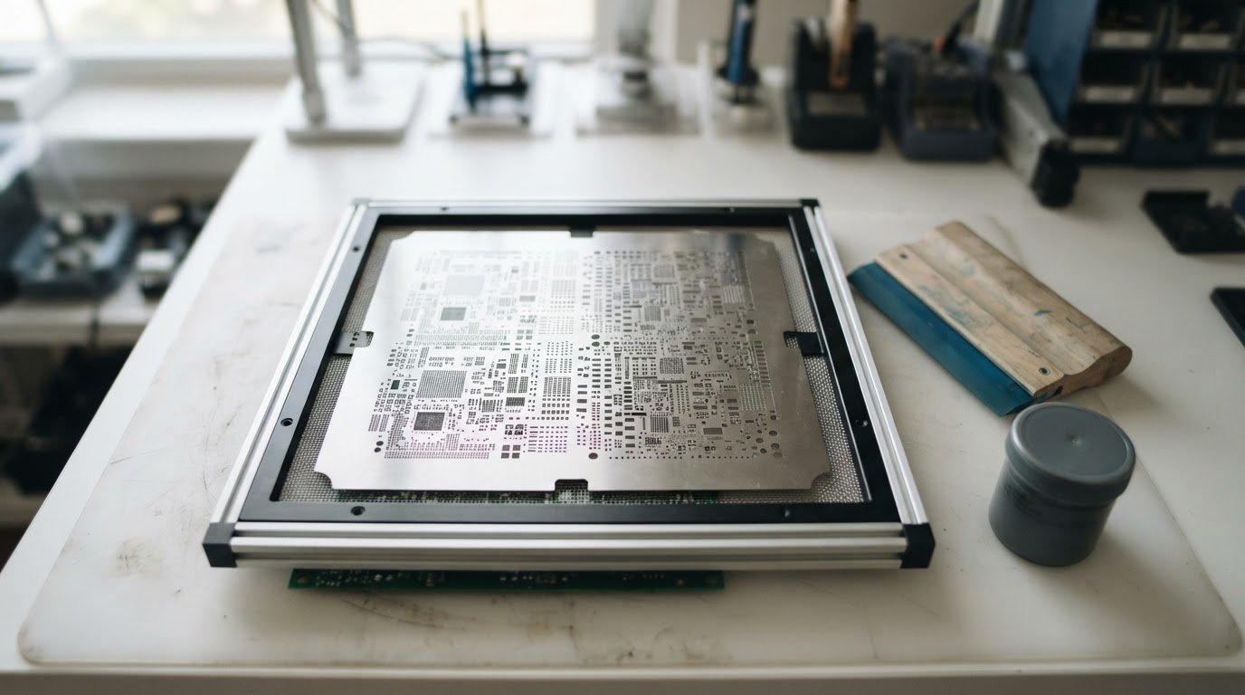
Every SMT assembly run requires a solder paste stencil. For FPGA boards with fine-pitch BGAs and QFPs, stencil quality directly impacts yield. Stencil types and their cost ranges in 2026:
- Frameless (prototype): $20–$60. Adequate for short runs; requires a universal frame.
- Framed stencil: $80–$200. Standard for production; reusable across multiple runs.
- Step stencil: $150–$400. Features multiple paste-deposit thicknesses for mixed-component boards—critical when you have 0.4 mm-pitch BGA alongside large QFN ground pads.
- Nano-coated stencil: Add $30–$80. Improves paste release for ultra-fine apertures.
Use the calculator below to estimate your stencil cost based on board size, stencil type, and thickness:
SMT Stencil Cost Estimator
Framed or frameless, plain laser or nano coated, and what each option is actually for.
How this is calculated
A framed stencil tensions properly and prints consistently across a long run. A frameless foil is cheaper and fine for a prototype in a manual printer, but it will not hold registration on an automatic line.
Electropolishing smooths the aperture walls so paste releases better, and nano coating goes further. Both are worth paying for when your worst area ratio is marginal, and wasted money when it is not. Check the area ratio first, then decide.
Stencil cost is relatively small compared to the bare board, but a poorly specified stencil causes bridging or insufficient solder on FPGA BGAs—leading to expensive rework. If you want to avoid common assembly pitfalls, review our guide on critical mistakes to avoid in FPGA assembly.
How FPGA Package Choice Impacts PCB Manufacturing Cost
The FPGA you select cascades into every cost driver above. Here’s a practical comparison:
| FPGA Package | Pitch | Typical Min Layers | HDI Required? | Relative PCB Cost |
|---|---|---|---|---|
| QFP-144 | 0.5 mm (lead) | 4 | No | Low |
| BGA-256 (1.0 mm) | 1.0 mm | 6 | Rarely | Moderate |
| BGA-484 (0.8 mm) | 0.8 mm | 8–10 | Usually | High |
| BGA-1156 (1.0 mm) | 1.0 mm | 12–16 | Sometimes | High |
| BGA-1760 (0.8 mm) | 0.8 mm | 16–20 | Yes | Very High |
When evaluating FPGAs from different vendors—whether you’re comparing Altera’s FPGA portfolio and availability against options from Gowin’s cost-effective FPGA series—always factor in the PCB cost delta between available packages. A $5 savings on the FPGA itself can easily be negated by a $15/board increase in fabrication cost due to a finer-pitch BGA.
7 Proven Strategies to Reduce PCB Manufacturing Cost
Strategy 1: Run a DFM Review Before Ordering
A thorough design-for-manufacturing review catches issues that inflate cost or cause yield loss—acid traps, starved thermals, annular ring violations, and more. Invest in a professional DFM review before you build to avoid expensive respins.
Strategy 2: Standardize Your Stackup
Fab houses maintain “standard” stackups that use materials they keep in stock. Designing to a standard stackup avoids minimum-order surcharges on exotic laminates and reduces lead time.
Strategy 3: Consolidate Via Types
Using through-hole vias wherever possible and limiting blind/buried vias to the BGA fan-out zone keeps HDI costs contained. Back-drilling is cheaper than buried vias for removing via stubs on high-speed channels.
Strategy 4: Optimize Panel Utilization
Work with your fabricator to adjust board outline dimensions by a few millimeters if it allows one more board per panel. On a 1,000-piece run, gaining one extra board per panel can save 5–8 % on total fabrication cost.
Strategy 5: Choose the Right Surface Finish
Don’t default to ENEPIG when ENIG will do. If your board has no wire-bonding requirements, ENIG provides excellent BGA solderability at lower cost.
Strategy 6: Plan Assembly and Fabrication Together
Turnkey services that bundle bare-board fabrication with component placement often negotiate better panel pricing. Explore turnkey FPGA PCB assembly with BGA and SMT services to consolidate your supply chain and reduce overhead.
Strategy 7: Source Components Early
Component shortages don’t just delay assembly—they force last-minute board redesigns when alternate parts have different footprints. Locking in your genuine FPGA and component sourcing early prevents costly PCB revisions.
PCB Manufacturing Cost Breakdown: A Real-World Example
Let’s walk through a realistic 2026 cost breakdown for a mid-complexity FPGA board:
- Design: 10-layer, 120 × 90 mm, 1+8+1 HDI stackup
- Material: Megtron 4 (mid-loss) core, FR-4 prepreg
- Features: 4/4 mil trace/space, ENIG finish, 4 controlled-impedance classes
- Quantity: 50 pieces
| Cost Component | Estimated Cost | % of Total |
|---|---|---|
| Base fabrication (10 layers) | $1,800 | 38 % |
| HDI processing (1+N+1) | $720 | 15 % |
| Specialty laminate upcharge | $540 | 11 % |
| Fine-line imaging (4/4 mil) | $380 | 8 % |
| ENIG surface finish | $310 | 7 % |
| Impedance testing (4 classes) | $260 | 5 % |
| Electrical testing (flying probe) | $350 | 7 % |
| Tooling and NRE | $280 | 6 % |
| Shipping | $120 | 3 % |
| Total (50 pcs) | $4,760 | 100 % |
| Per-board cost | ~$95 |
At 500 pieces, the same board drops to roughly $28–$35 each as NRE amortizes and panel utilization improves. At 5,000 pieces, expect $12–$18. These numbers illustrate why volume planning is essential to managing PCB manufacturing cost effectively.
2026 Trends Affecting PCB Manufacturing Cost
Copper prices remain elevated, adding 5–10 % to boards with 2 oz+ copper planes common in FPGA power delivery. Sustainability regulations in the EU are pushing fabricators toward halogen-free laminates, which carry a modest premium today but are expected to reach cost parity by late 2026. AI-driven DFM tools are shortening the quote-to-production cycle, reducing NRE for complex boards. Finally, substrate-like PCB (SLP) technology—already common in smartphones—is beginning to appear in FPGA prototyping for chiplet-based devices, though at a significant cost premium.
Frequently Asked Questions About PCB Manufacturing Cost
What is the average PCB manufacturing cost for an FPGA prototype?
For a typical 8-to-10-layer FPGA prototype board (100 × 100 mm, ENIG finish, controlled impedance), expect to pay $80–$250 per board when ordering 1–5 pieces. Adding HDI features for fine-pitch BGAs can push that figure to $150–$400 per board. Costs drop sharply once you move to pilot quantities of 10–50 pieces.
How does layer count affect PCB manufacturing cost?
Layer count is the single biggest cost multiplier. A 4-layer board costs roughly 1.8–2.2× what a 2-layer board costs, while a 16-layer board can run 5–9× higher. Each additional pair of layers adds lamination, drilling, and imaging steps. FPGA designers should audit pin assignments and consider package alternatives to minimize the required layer count.
Can I reduce PCB manufacturing cost without sacrificing signal integrity?
Yes. The most effective approaches include standardizing your stackup to use in-stock materials, consolidating impedance classes to reduce testing overhead, using hybrid laminates instead of full low-loss substrates, and optimizing panel utilization. A professional DFM review often identifies 15–25 % in savings that don’t compromise electrical performance.
How much do rush orders add to PCB manufacturing cost?
Rush fabrication with 24–48 hour turnaround typically adds 100–300 % to the standard prototype price. Even a modest acceleration from 10-day to 5-day delivery can add 30–60 %. Planning your design schedule to avoid expedite fees is one of the simplest ways to control your overall budget.
Final Thoughts
PCB manufacturing cost is not a single number—it’s the sum of dozens of engineering decisions made during FPGA selection, schematic design, and board layout. By understanding which factors carry the most weight and applying the strategies outlined above, you can often reduce your per-board cost by 20–40 % without compromising signal integrity or reliability. Start with the FPGA package, design to a standard stackup, run a DFM check, and plan your volumes realistically. Your budget—and your production schedule—will thank you.