
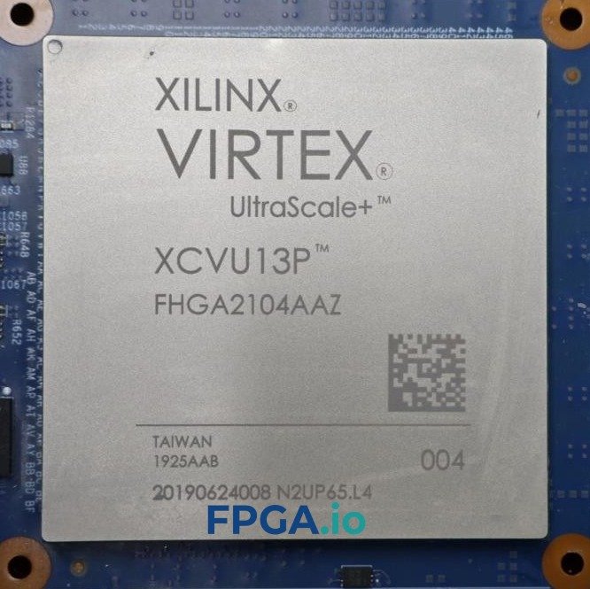

Description
What the XCVU9P-2FLGB2104I Is Built For
The XCVU9P-2FLGB2104I sits at the top of AMD Xilinx’s Virtex UltraScale+ line. It uses stacked silicon interconnect (SSI) to join three super logic regions (SLRs) into a single device, which is how it reaches 2.59 million system logic cells in one package. Designs that outgrow a monolithic FPGA — 8K video pipelines, ASIC emulation platforms, network processing at 100GbE — land here.
XCVU9P-2FLGB2104I Key Specifications
| Parameter | Value |
|---|---|
| Device family | Virtex UltraScale+ (VU9P) |
| Process | 16nm FinFET+ |
| System logic cells | 2,586,150 |
| CLB LUTs / flip-flops | 1,182,240 / 2,364,480 |
| Block RAM | 2,160 × 36Kb (75.9Mb) |
| UltraRAM | 960 × 288Kb (270Mb) |
| DSP slices | 6,840 |
| GTY transceivers | Up to 120, 32.75 Gb/s (device max) |
| Hard IP | PCIe Gen3 x16, 100G Ethernet MAC/PCS, 150G Interlaken |
| Speed grade | -2 |
| Temperature grade | Industrial, -40°C to +100°C (Tj) |
| Package | FLGB2104, 2,104-ball FCBGA, 47.5 × 47.5mm, 1.0mm pitch |
| RoHS | Compliant (Pb-free) |
How to Read the XCVU9P-2FLGB2104I Part Number
- XC — AMD Xilinx commercial product prefix
- VU9P — Virtex UltraScale+, device size 9P
- -2 — speed grade (mid-tier; -1, -2, -3 available)
- FLG — flip-chip lidded, Pb-free package
- B2104 — package variant B, 2,104 balls
- I — industrial temperature grade
Order the wrong final letter and you get the extended-temperature (E) part instead, which is not a drop-in for industrial qualification paperwork even though the die is identical.
FLGB2104 Package and PCB Design Notes
At 47.5 × 47.5mm on a 1.0mm pitch, this package needs a high-layer-count board with controlled-impedance routing for the GTY lanes. Plan for a stiffener or backing plate: large lidded FCBGAs are sensitive to board flex during reflow and in-system. Power delivery is the other constraint — VCCINT current on a fully utilized VU9P runs high enough that PDN impedance, not logic timing, is often what limits the design.
Why -2 Speed and Industrial Grade
The -2 grade is the volume choice for this device. It gives meaningful Fmax headroom over -1 without the price and availability penalty of -3. The industrial rating extends the junction temperature floor to -40°C, which matters for outdoor 5G radio units, rail, and test equipment that cold-starts.
Design Tools and IP Support
The VU9P requires Vivado ML Enterprise Edition — it is not covered by the free Standard edition licence. Budget for that before quoting a project. Vitis, the UltraScale+ Memory IP for DDR4, and the integrated 100G Ethernet subsystem are all supported. When partitioning across SLRs, place Laguna registers deliberately; automatic SLR crossings are the most common source of timing closure failures on this device.
Applications
- Data center and cloud FPGA acceleration
- ASIC prototyping and hardware emulation
- 5G massive MIMO and baseband processing
- 100G/400G network packet processing
- Machine learning inference offload
- High-end test, measurement, and defense signal processing
XCVU9P-2FLGB2104I FAQ
How is the XCVU9P-2FLGB2104I different from the XCVU9P-2FLGB2104E?
Same silicon, same package, different temperature qualification. The I part is rated -40°C to +100°C junction; the E part is 0°C to +100°C. Choose I for industrial, outdoor, or automotive-adjacent environments.
What is the difference between FLGB2104 and FLGA2104?
Both are 2,104-ball packages with the same body size, but the A and B variants bond out different mixes of user I/O and GTY transceivers. They are not pin-compatible — confirm against the datasheet before reusing a layout.
How many SLRs does the VU9P have?
Three. The device is an SSI part, so cross-SLR paths carry extra latency and need Laguna register placement to close timing.
Does it support PCIe Gen3 x16?
Yes, through integrated hard blocks, alongside 100G Ethernet MAC/PCS and 150G Interlaken cores.
Is it RoHS compliant?
Yes. The G in FLGB indicates a Pb-free, RoHS-compliant package.
Order the XCVU9P-2FLGB2104I
Contact FPGA.io for current pricing, stock, and lead time on the XCVU9P-2FLGB2104I, including partial-reel and single-unit quantities.
Reviews
There are no reviews yet.